Wide gap semiconductor device and method for manufacturing same

a semiconductor device and wide gap technology, applied in semiconductor devices, diodes, electrical devices, etc., can solve the problems of difficulty in sufficiently reducing the electric field at the interface between the schottky electrode and the substrate, and achieve the effect of wide gap, reducing the surface utilization percentage of electron emission during forward voltage application, and eliminating damage at the side face of the trench

Inactive Publication Date: 2014-03-06
SUMITOMO ELECTRIC IND LTD
View PDF2 Cites 24 Cited by
  • Summary
  • Abstract
  • Description
  • Claims
  • Application Information

AI Technical Summary

Benefits of technology

[0016]According to the method for manufacturing a wide gap semiconductor device according to the present invention, there is manufactured a wide gap semiconductor device having a Schottky electrode adjoining the first-conductivity-type region at the side face of the trench and the main face, and adjoining the second-conductivity-type region at the bottom of the trench. Accordingly, by increasing the electric field of the second-conductivity-type region during application of backward voltage, the electric field at the interface between the Schottky electrode and the first-conductivity-type region can be alleviated.
[0017]According to a method for manufacturing a wide gap semiconductor device according to the present invention, there is manufactured a wide gap semiconductor device having the side face of the trench inclined relative to the main face of the substrate. Accordingly, the area of contact between the Schottky electrode and the first-conductivity-type region can be increased as compared to the case where the side face of the trench is parallel to the main face of the substrate. As a result, a current path can be ensured since the surface utilization percentage of electron emission during application of forward voltage is increased.
[0018]Preferably in the method for manufacturing a wide gap semiconductor device set forth above, the step of forming a trench is performed by thermal etching. Accordingly, the damage at the side face of the trench can be eliminated.
[0019]According to the present invention, there can be provided a wide gap semiconductor device allowing the electric field at the interface between a Schottky electrode and substrate to be alleviated effectively, and a method for manufacturing the wide gap semiconductor device.

Problems solved by technology

However, it was difficult to sufficiently reduce the electric field at the interface between the Schottky electrode and substrate in the Schottky diodes disclosed in Japanese Patent Laying-Open No. 2001-85704 and Japanese Patent Laying-Open No. 2009-16603.

Method used


Image

  • Wide gap semiconductor device and method for manufacturing same
  • Wide gap semiconductor device and method for manufacturing same
  • Wide gap semiconductor device and method for manufacturing same

Examples


first embodiment

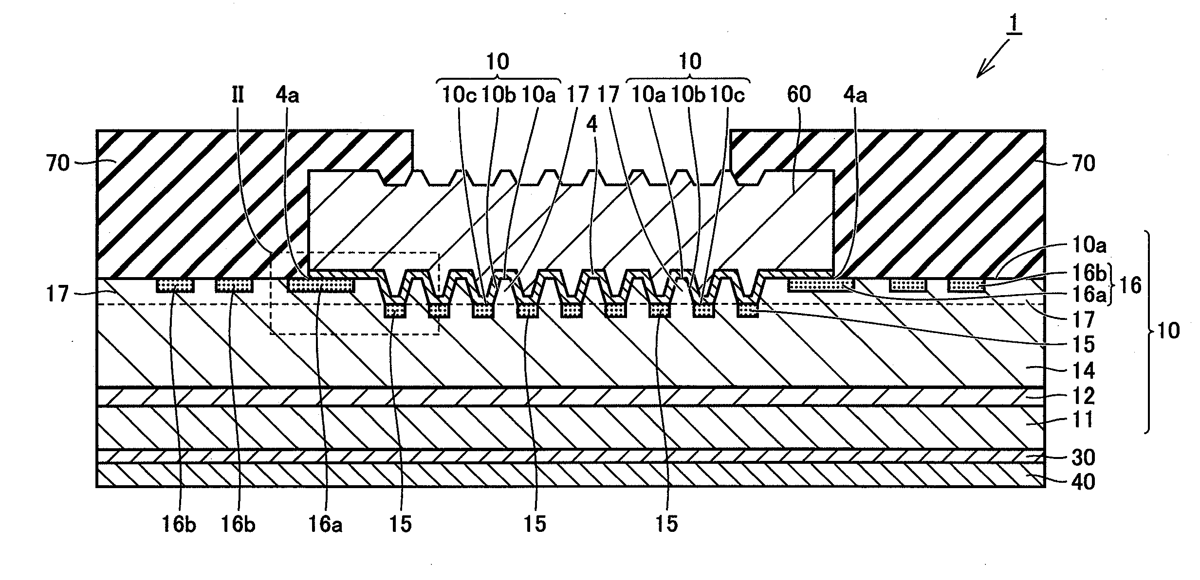
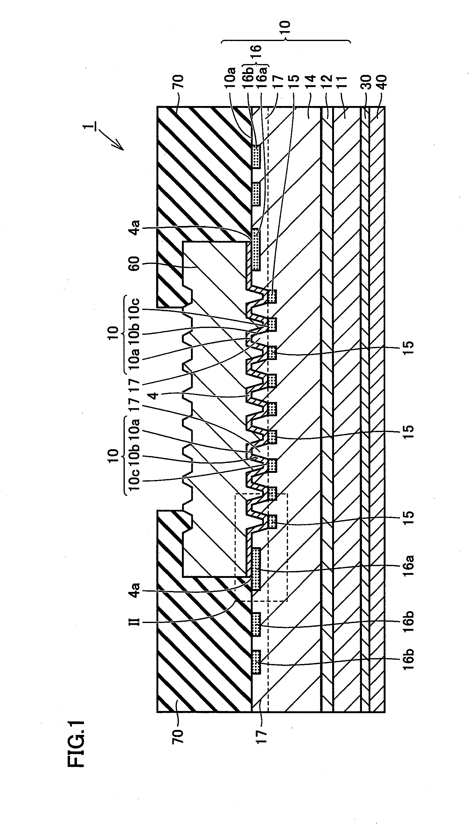
[0034]First, a configuration of a Schottky barrier diode 1 that is a wide gap semiconductor device according to a first embodiment of the present invention will be described with reference to FIG. 1. As shown in FIG. 1, Schottky barrier diode 1 of the present embodiment mainly includes a substrate 10, a Schottky electrode 4, and an ohmic electrode 30. Substrate 10 is formed of a wide gap semiconductor material, and has a main face 10a. The wide gap semiconductor material refers to a semiconductor material having a band gap greater than that of silicon. Specifically, silicon carbide, gallium nitride, and diamond can be cited as the wide gap semiconductor material.

[0035]Substrate 10 includes an n+ substrate 11, an electric field termination layer 12, an n type region 17, a junction termination extension (JTE) region 16, and a p type region 15. N+ substrate 11 corresponds to a substrate formed of single crystal silicon carbide, containing impurities such as nitrogen (N). The impurity c...

second embodiment

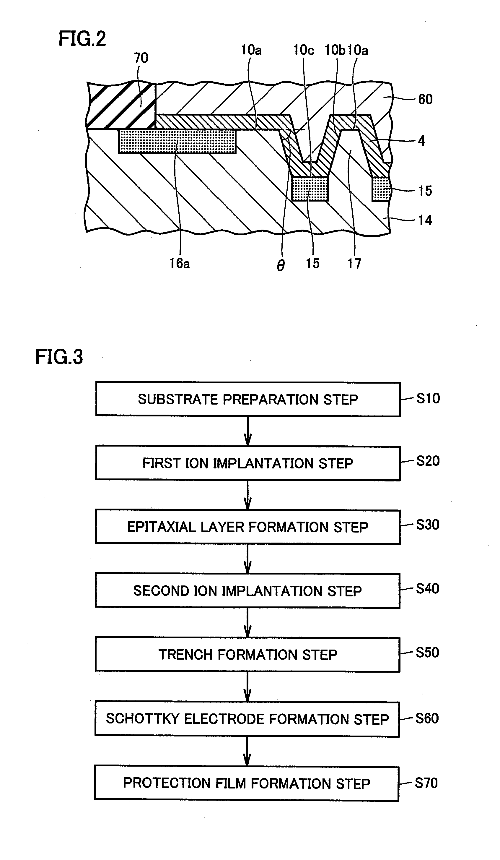
[0063]A configuration of Schottky barrier diode 1 that is a wide gap semiconductor device according to a second embodiment of the present invention will be described with reference to FIG. 10. Schottky barrier diode 1 of the second embodiment differs from Schottky barrier diode 1 of the first embodiment in that there is provided a first p type region 16a adjoining Schottky electrode 4 and a second p type region 16b not adjoining Schottky electrode 4. The remaining elements are similar to those of Schottky barrier diode 1 of the first embodiment.

[0064]Referring to FIGS. 10 and 11, Schottky barrier diode 1 of the second embodiment includes a first trench 2a and a second trench 2b adjacent to each other. P type region 15 includes a first p type region 15a (first second-conductivity-type region) adjoining bottom 10c of first trench 2a, a second p type region 15b (second second-conductivity-type region) adjoining bottom 10c of second trench 2b, and a third p type region 15c (third second...


PUM


Abstract

A wide gap semiconductor device includes a substrate and a Schottky electrode. The substrate formed of a wide gap semiconductor material has a main face, and includes a first-conductivity-type region and a second-conductivity-type region. The Schottky electrode is arranged adjoining the main face of the substrate. At the substrate, there is foamed a trench having a side face continuous with the main face and a bottom continuous with the side face. The Schottky electrode adjoins the first-conductivity-type region at the side face of the trench and the main face, and adjoins the second-conductivity-type region at the bottom of the trench. The side face of the trench is inclined relative to the main face of the substrate.

Description

BACKGROUND OF THE INVENTION[0001]1. Field of the Invention[0002]The present invention relates to a wide gap semiconductor device, and a method for manufacturing a wide gap semiconductor device. More particularly, the present invention relates to a wide gap semiconductor device that can alleviate the electric field at the interface between a Schottky electrode and a substrate, and a method for manufacturing such a wide gap semiconductor device.[0003]2. Description of the Background Art[0004]Semiconductor devices such as a Schottky barrier diode (SBD) and junction barrier Schottky diode (JBS) have a configuration in which a Schottky electrode is formed on a substrate. Since the work function difference between metal qualified as the electrode material and semiconductor is small in a Schottky barrier diode, the leakage current during application of reverse voltage readily becomes great as compared to that of a PN diode. Therefore, various configurations are proposed in order to reduce ...

Claims


Application Information

Patent Timeline
Patent Type & Authority Applications(United States)
IPC IPC(8): H01L29/872H01L29/66
CPCH01L29/66143H01L29/872H01L29/0619H01L29/0623H01L29/1602H01L29/1608H01L29/2003H01L29/6603H01L29/6606H01L29/66212
Inventor WADA, KEIJIMASUDA, TAKEYOSHIHIYOSHI, TORU
Owner SUMITOMO ELECTRIC IND LTD
Why Eureka
Try Eureka