Methods And Apparatus For Forming Tantalum Silicate Layers On Germanium Or III-V Semiconductor Devices

a technology of germanium or iiiv semiconductor devices and gate dielectric layers, which is applied in the direction of coating, chemical vapor deposition coating, coating process, etc., can solve the problems of not meeting the requirements of tsub>inv/sub>, over-all power consumption is also increased,

Inactive Publication Date: 2014-03-06
APPLIED MATERIALS INC
View PDF6 Cites 189 Cited by
  • Summary
  • Abstract
  • Description
  • Claims
  • Application Information

AI Technical Summary

Benefits of technology

[0006]One aspect of the current invention relates to a method of processing a substrate to provide a tantalum silicate layer on a surface of the substrate. In various embodiments the method comprises depositing a silicon oxide layer on the substrate, depositing a tantalum oxide layer on the silicon oxide layer; and diffusing the tantalum oxide layer into the silicon oxide layer to provide a tantalum silicate layer. In one or more embodiments, the tantalum silicate layer has a Si / (Ta+Si) ratio in the range from about 0.01 to about 0.15. In some embodiments, the Si / (Ta+Si) ratio is in the range from about 0.03 to about 0.10. The substrate may have a germanium or III-V semiconductor surface.

Problems solved by technology

However, as CMOS technology is continuously miniaturized and the transistor count exponentially rises, overall power consumption is also increased, making performance per watt of energy consumption a key figure-of-merit for today's performance microprocessors.
However, current gate stack materials do not meet these requirements for Tinv.

Method used


Image

  • Methods And Apparatus For Forming Tantalum Silicate Layers On Germanium Or III-V Semiconductor Devices
  • Methods And Apparatus For Forming Tantalum Silicate Layers On Germanium Or III-V Semiconductor Devices
  • Methods And Apparatus For Forming Tantalum Silicate Layers On Germanium Or III-V Semiconductor Devices

Examples


Embodiment Construction

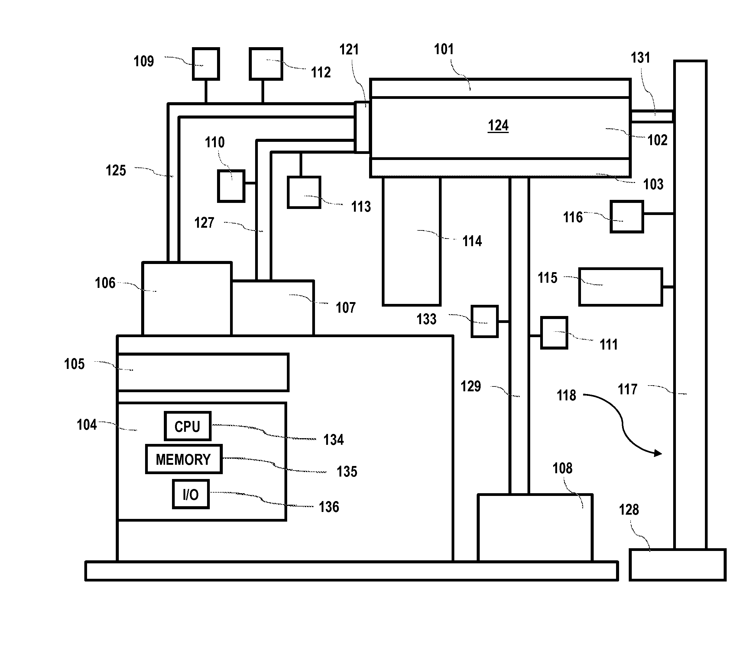
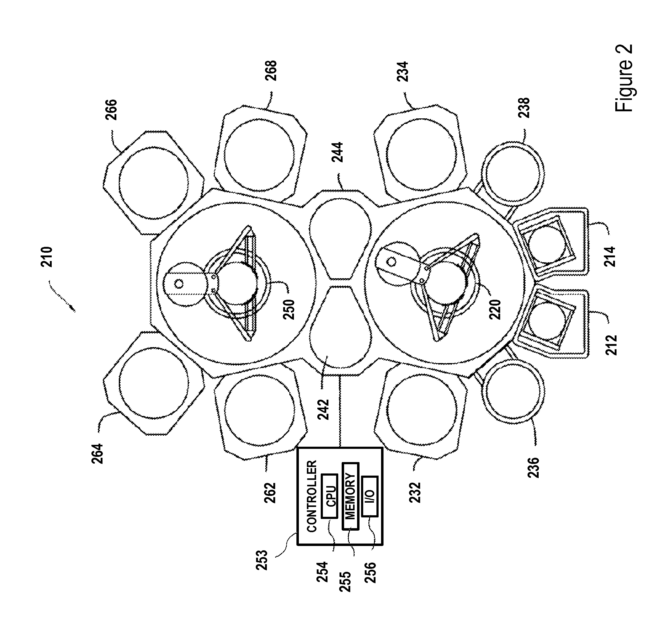
[0022]In order to avoid the drawbacks of other gate stack materials, new methods of forming gate stack materials for Ge and III-V semiconductor devices are provided. Specifically, embodiments of the invention provide methods and apparatus for forming Ta-rich TaSiOx layers for Ge and III-V semiconductor devices. TaSiOx may be used as a common gate dielectric for Ge and III-V materials, thus enabling high performance / low power CMOS devices that use Ge channel p-MOSFET and III-V channel n-MOSFET.

[0023]Silicon and silicon dioxide (SiO2) are both candidate materials for the interfacial layer between the Ge or III-V materials and the high-k dielectric. However, as atomic layer deposition (ALD) of silicon is difficult on substrates having Ge and III-V surfaces, embodiments of the present invention pertain to the deposition of SiO2, which is easier to deposit than pure silicon films.

[0024]Furthermore, hafnium dioxide (HfO2) and tantalum pentoxide (Ta2O5) have similar dielectric constants, b...


PUM

PropertyMeasurementUnit
thicknessaaaaaaaaaa
temperatureaaaaaaaaaa
inversion layer thicknessaaaaaaaaaa

Abstract

Described are apparatus and methods for forming tantalum silicate layers on germanium or III-V materials. Such tantalum silicate layers may have Si/(Ta+Si) atomic ratios from about 0.01 to about 0.15. The tantalum silicate layers may be formed by atomic layer deposition of silicon oxide and tantalum oxide, followed by interdiffusion of the silicon oxide and tantalum oxide layers.

Description

CROSS-REFERENCE TO RELATED APPLICATIONS[0001]This application claims the benefit under 35 U.S.C. §119(e) to U.S. Provisional Application No. 61 / 693,856, filed Aug. 28, 2012, the entire contents of which are incorporated herein by reference in their entirety.FIELD[0002]Embodiments of the present invention generally relate to the field of semiconductor manufacturing processes and devices, particularly to methods and apparatus for forming gate dielectric layers on Ge or III-V semiconductor devices.BACKGROUND[0003]Microelectronic devices are fabricated on a semiconductor substrate as integrated circuits in which various conductive layers are interconnected with one another to permit electronic signals to propagate within the device. An example of such a device is a complementary metal-oxide-semiconductor (CMOS) field effect transistor (FET) or MOSFET.[0004]An exemplary FET or MOSFET includes a gate electrode on a gate dielectric layer on a surface of a silicon substrate. However, as CMO...

Claims


Application Information

Patent Timeline
Patent Type & Authority Applications(United States)
IPC IPC(8): H01L21/02
CPCH01L21/02225H01L21/0215C23C16/401C23C16/405C23C16/45529C23C16/45531C23C16/45536C23C16/56H01L21/0228H01L21/28255H01L21/28264
Inventor ANTHIS, JEFFREY W.AHMED, KHALED Z.
Owner APPLIED MATERIALS INC
Why Eureka
Try Eureka