Wavelength conversion element, method of manufacturing the same, and LED element and semiconductor laser light emitting device using wavelength conversion element

a technology of wavelength conversion element and semiconductor laser, which is applied in semiconductor lasers, lighting and heating devices, instruments, etc., can solve the problems of liable deterioration of silicon resin, and achieve the effects of reducing the risk of deterioration, and increasing the resistance to ultraviolet radiation

Active Publication Date: 2014-03-13
PANASONIC CORP
View PDF5 Cites 60 Cited by
  • Summary
  • Abstract
  • Description
  • Claims
  • Application Information

AI Technical Summary

Benefits of technology

[0012]A conventional wavelength conversion element for a light emitting element is required to have higher optical output, higher resistance to heat, and higher resistance to ultraviolet radiation. Hon-limiting and exemplary embodiments of the present application provide a wavelength conversion element having high optical output, high resistance to heat, and nigh resistance to ultraviolet radiation, a method of manufacturing the same, and an LED element and a semiconductor laser light emitting device using the same.
[0014]According to a technique disclosed in the present application, by using zinc oxide which is an inorganic matrix having a high refractive index, high resistance to heat, and high resistance to ultraviolet radiation, light scattering in a phosphor layer is reduced. Thus, the LED element, the semiconductor laser light emitting device, and the phosphor layer having high optical output can be realized.

Problems solved by technology

However, when a large current is passed through a high-brightness LED chip which is commercialized in recent years, the silicone resin is liable to be deteriorated by heat and high-brightness ultraviolet radiation generated from the LED chip.

Method used


Image

  • Wavelength conversion element, method of manufacturing the same, and LED element and semiconductor laser light emitting device using wavelength conversion element
  • Wavelength conversion element, method of manufacturing the same, and LED element and semiconductor laser light emitting device using wavelength conversion element
  • Wavelength conversion element, method of manufacturing the same, and LED element and semiconductor laser light emitting device using wavelength conversion element

Examples


embodiment 1

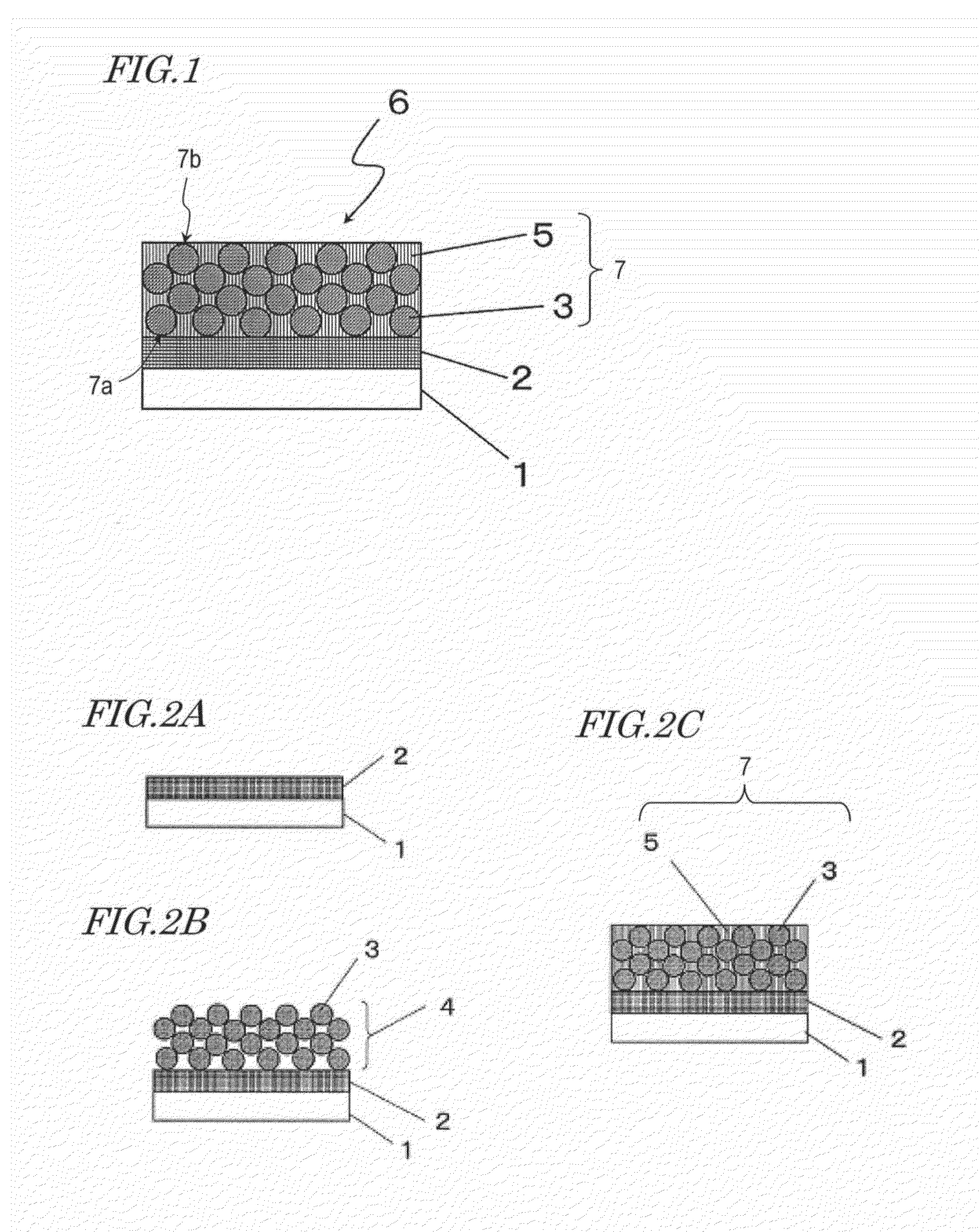
[0102]FIG. 1 is a sectional view of a wavelength conversion element of Embodiment 1.

[0103]A wavelength conversion element 6 of this embodiment includes a phosphor layer 7 which itself includes a plurality of phosphor particles 3 and a matrix 5 located among the plurality of phosphor particles 3. The wavelength conversion element 6 converts at least a part of incident light info light in a wavelength band which is different from the wavelength band of the incident light and emits the converted light.

[0104]As the plurality of phosphor particles 3, a phosphor having various excitation wavelengths, exiting light wavelengths, and particle diameters ordinarily used for a light emitting element can be used. For example, YAG (yttrium aluminum garnet), β-SiAlON, or she like can be used. In particular, the wavelength for exciting the phosphor and the wavelength of exiting light can be arbitrarily selected in accordance with the use of the wavelength conversion element 6. Further, in accordanc...

embodiment 2

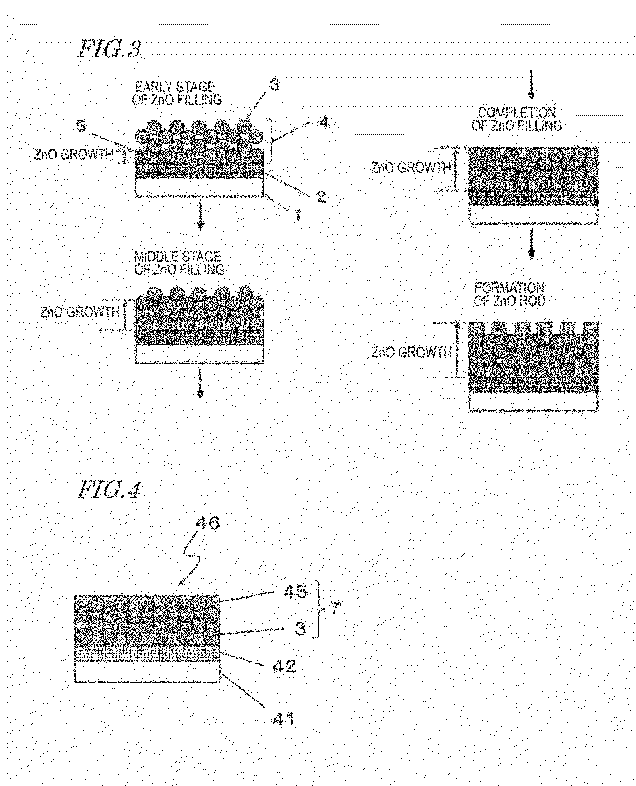
[0126]FIG. 4 is a sectional view of a wavelength conversion element according to Embodiment 2.

[0127]A wavelength conversion element 46 according to this embodiment includes a substrate 41, a thin film 42, and a phosphor layer 7′. The substrate 41 is a single crystalline substrate, and the thin film 42 is termed of single crystalline zinc oxide. Further, in the phosphor layer 7′, a matrix 45 is formed of single crystalline zinc oxide.

[0128]In Embodiment 2, voids in the phosphor particle layer 4 formed of the phosphor particles 3 are filled with single crystalline zinc oxide which is crystal grown from the thin film 42 of single crystalline zinc oxide.

[0129]According to the wavelength conversion element of this embodiment, the matrix 45 is formed of single crystalline zinc oxide, and thus, the number of the grain boundaries in the matrix 45 is further reduced so that scattering of light which enters the phosphor layer is further reduced. Therefore, the wavelength conversion element ac...

embodiment 3

[0136]FIG. 6A is a sectional view of a wavelength conversion element according to Embodiment 3.

[0137]A wavelength conversion element 200 according to this embodiment includes a substrate 210, a thin film 220, a phosphor layer 230, and a two-dimensional periodic structure 240. The substrate 210 includes a support 211 and a reflective layer 212. As the support 211, for the purpose of efficiently discharge heat generated in phosphor particles 231, a material having a high thermal conductivity such as a metal, for example, aluminum, or ceramic can be used. As the reflective layer 212, a material which reflects light of a visible wavelength including fluorescence can be used, and, from the viewpoint of discharging heat, a metal such as aluminum or sliver can be used.

[0138]The thin film 220 is, similarly to the cases of Embodiments 1 and 2, formed of polycrystalline or single crystalline zinc oxide.

[0139]The phosphor layer 230 includes, similarly to the cases of Embodiments 1 and 2, a mat...


PUM

PropertyMeasurementUnit
refractive indexaaaaaaaaaa

Abstract

A wavelength conversion element disclosed in the present application includes a phosphor layer including a plurality of phosphor particles and a matrix that is located among the plurality of phosphor particles and is formed of zinc oxide. The zinc oxide is columnar crystals or a single crystal in a c-axis orientation.

Description

[0001]This is a continuation of International Application No. PCT / JP2013 / 003103, with an international filing date of May 15, 2013, which claims priorities of Japanese Patent Application No. 2012-112163, filed on May 16, 2012, Japanese Patent Application No. 2012-113250, filed, on May 17, 2012 and Japanese Patent Application No. 2012-116188, filed on May 22, 2012, the contents of which are hereby incorporated by reference.BACKGROUND[0002]1. Technical Field[0003]The present application relates to a wavelength conversion element including phosphor particles and a method of manufacturing she some, and an LED element and a semiconductor laser light emitting device using the same.[0004]2. Description of the Related Art[0005]In recent years, a light emitting diode (LED) has come into use for lighting, and a higher-brightness and longer-life LED is desired to be developed. Conventionally, a wavelength conversion element including a phosphor layer for a white LED is forced by curing a resin...

Claims


Application Information

Patent Timeline
Patent Type & Authority Applications(United States)
IPC IPC(8): F21K99/00C09K11/08H01L33/50
CPCF21K9/56C09K11/08H01L33/502H01L33/50H01L33/486H01L33/501H01L2224/48091H01L2224/73265H01S5/005H01S5/02257H01L2924/00014F21K9/64G03B21/204G03B33/06G03B33/12H01L2924/16195H01L2924/3025H01S5/02212H01S5/32341H05B33/10H01S5/0087H01L2924/00G03B21/14
Inventor HAMADA, TAKAHIROSUZUKI, NOBUYASUORITA, KENJINAGAO, NOBUAKI
Owner PANASONIC CORP
Why Eureka
Try Eureka