Method and System for Operating Semiconductor Optical Amplifiers

a semiconductor optical amplifier and optical amplifier technology, applied in semiconductor lasers, nanotechnology, laser details, etc., can solve the problems of increasing the cost and complexity of drive electronics, requiring high power and high frequency acoustic signals, and reducing the efficiency of semiconductor lasers, so as to improve the modulator extinction

Inactive Publication Date: 2014-03-13
INNOVATIVE PHOTONIC SOLUTIONS INC
View PDF2 Cites 6 Cited by
  • Summary
  • Abstract
  • Description
  • Claims
  • Application Information

AI Technical Summary

Benefits of technology

[0009]Disclosed is a method for using a semiconductor optical amplifier as an optical modulator for pulsed signals. In accordance with the principles of the invention, the SOA can be biased with a negative voltage to suppress transmission in the absence of a pulse and improve the modulator extinction. A positive pulsed signal is applied with sufficient amplitude to forward bias the amplifier, both transmitting the carrier and increasing its amplitude by means of the gain provided by the SOA under forward biased conditions.

Problems solved by technology

However there has been minimal work done in the area of applying SOAs to operate as modulators for other applications and much of that previous work has been related to phase modulation.
For other applications, such as coherent imaging, however, high extinction ratio and narrow linewidth are critical and involve operating the SOA under large signal conditions while still minimizing the “chirp” added to the linewidth by the amplifier.
The disadvantage of AOMs is that they require high power and high frequency acoustic signals to allow high speed modulation.
These factors increase the cost and complexity of the drive electronics.
Additionally, AOMs can be bulky and hard to utilize in miniaturized systems.
However, because of the need to couple light in and out of the edges of the waveguide, they can have high coupling losses.
In addition, the extinction coefficient of EAMs is typically not very high, reaching approximately 11 dB for waveguide devices with high RF bandwidths (Id.).
Mach Zehnder or other interferometer style amplitude modulators suffer from the same issues, plus the chip designs are typically more complex; requiring multiple waveguides and branching and combining junctions.

Method used


Image

  • Method and System for Operating Semiconductor Optical Amplifiers
  • Method and System for Operating Semiconductor Optical Amplifiers
  • Method and System for Operating Semiconductor Optical Amplifiers

Examples


Embodiment Construction

[0021]Before the present devices, systems and methods are described, it is to be understood that this invention is not limited to the particular processes, devices, or methodologies described, as these may vary. It is also to be understood that the terminology used in the description is for the purpose of describing the particular versions or embodiments only and is not intended to limit the scope of the present disclosure which will be limited only by the appended claims.

[0022]Certain terms are defined in this section to facilitate understanding of exemplary embodiments.

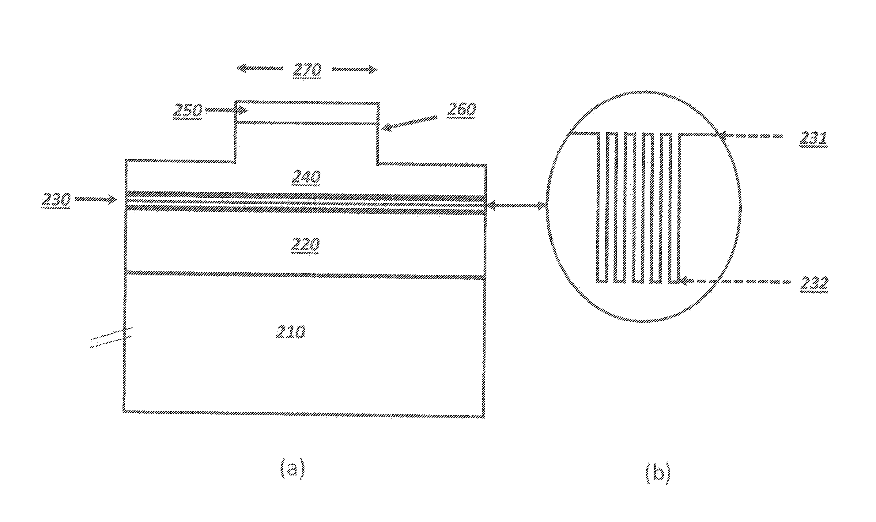
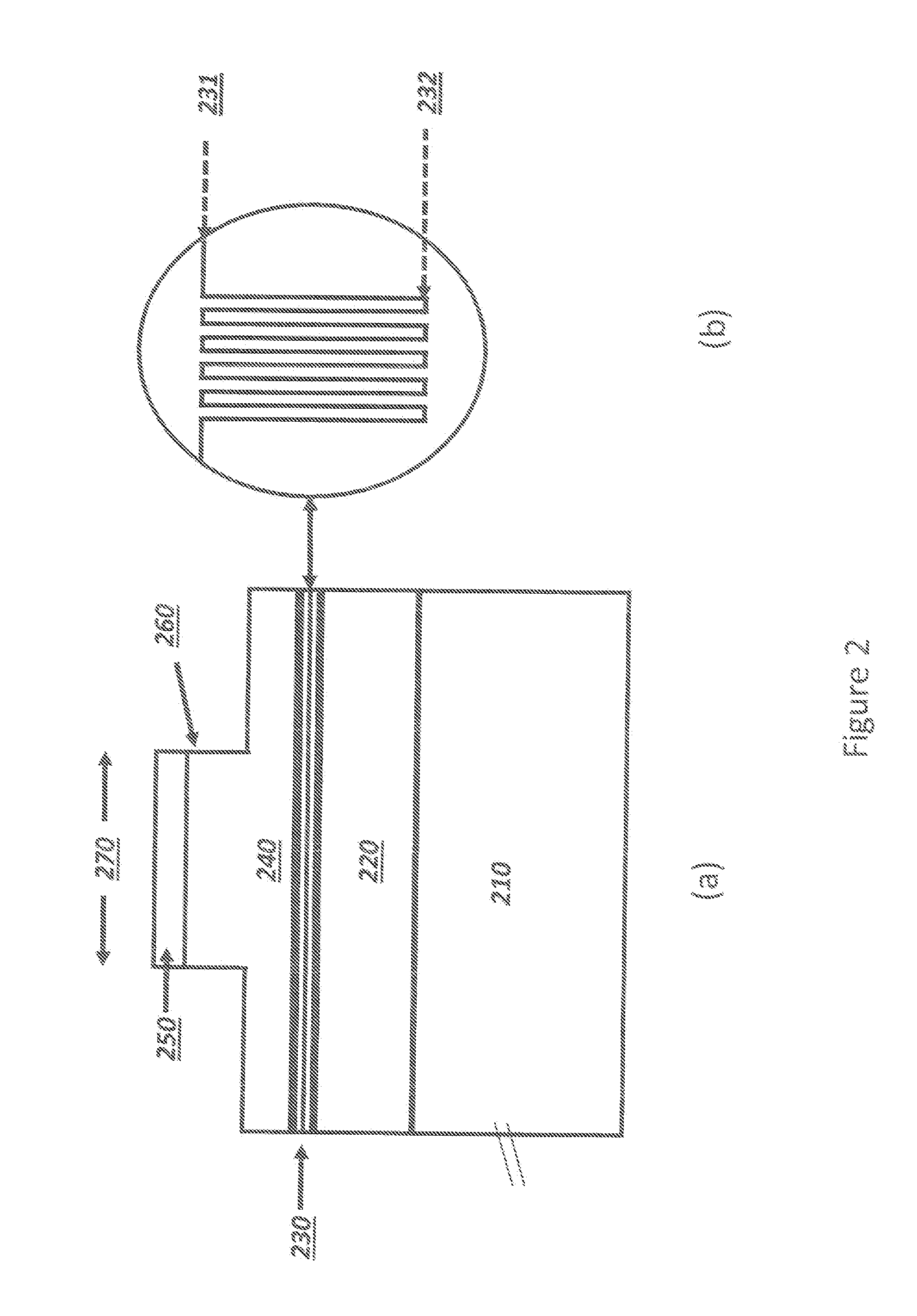
[0023]A semiconductor optical amplifier (SOA) provides optical gain, typically embodied in a layered semiconductor structure that incorporates a waveguide that transmits light from the entrance facet of the device to the exit facet. The semiconductor optical amplifier is typically excited by injection of electrons and holes through electrical contacts. The facets of the semiconductor optical amplifier are often prov...


PUM


Abstract

Disclosed are systems and methods for using a semiconductor optical amplifier (SOA) as an optical modulator for pulsed signals. In accordance with the principles of the invention, the SOA can be biased with a negative voltage to suppress transmission and improve modulator extinction and biased with a positive pulsed signal with sufficient amplitude to forward bias the amplifier (SOA), both transmitting the carrier and increasing its amplitude by means of a gain provided by the SOA under forward biased conditions. In addition, the forward bias voltage may be selected to compensate for losses within the SOA.

Description

CLAIM OF PRIORITY[0001]This application claims, pursuant to 35 USC 119, priority to and the benefit of the earlier filing date to that U.S. Provisional Application Ser. No. 61 / 700,237, entitled, “Method for Operating Semiconductor Optical Amplifiers as Modulators,” filed Sep. 12, 2012. The entire content of the above-referred-to application is incorporated, herein, by reference in its entirety.FIELD OF THE INVENTION[0002]This invention relates to semiconductor optical amplifiers and, more particularly, to semiconductor optical amplifiers which are negatively biased and driven by positive voltage pulses.BACKGROUND[0003]Semiconductor Optical Amplifiers (SOAs) have been shown to operate as modulators in applications for fiber optical communications. However there has been minimal work done in the area of applying SOAs to operate as modulators for other applications and much of that previous work has been related to phase modulation. For example, Mørk et al. (The Modulation Response of ...

Claims


Application Information

Patent Timeline
Patent Type & Authority Applications(United States)
IPC IPC(8): H01S5/00
CPCH01S5/0085H01S5/0014H01S5/0078H01S5/0428H01S5/06226H01S5/1085H01S5/22H01S5/34313H01S5/4006H01S5/50B82Y20/00
Inventor CONNOLLY, JOHN C.ACKLEY, DONALD E.RUDDER, SCOTT L.GUENTHER, HARALD R.
Owner INNOVATIVE PHOTONIC SOLUTIONS INC
Why Eureka
Try Eureka