Solar Cell Having Selective Emitter

a selective emitter and solar cell technology, applied in the field of solar cells, can solve the problems of harming readily-made textured surfaces, methods that are not yet fit for mass production, and are not suitable for mass production, and achieve the effect of lowering the concentration of doping

Inactive Publication Date: 2014-03-13
NATIONAL TSING HUA UNIVERSITY
View PDF6 Cites 15 Cited by
  • Summary
  • Abstract
  • Description
  • Claims
  • Application Information

AI Technical Summary

Benefits of technology

[0006]The second method processes a heavy doping process all over the surface at the illuminated side of a silicon substrate to form a heavily-doped diffusion layer. Then, a barrier is formed through screen-printing for obtaining lightly- and heavily-doped diffusion regions with the coordination of an etching-back process. This method requires uniform etching-back at a large area with high complexity, which is not fit for mass production and may even harm readily-made textured surface during etching-back. Besides, the solar cell thus made requires high-precision aligning device for printing silver paste on the heavily-doped diffusion region. A light-induced plating process is required to increase the thickness of silver wires and reduce resistance of the silver wires. Hence, this method is not yet fit for mass production.
[0011]To achieve the purpose above, the present invention is a solar cell having a selective emitter, wherein the solar cell is fabricated by using a pre-doped silicon substrate; the silicon substrate is a mono-crystalline silicon substrate or a multi-crystalline silicon substrate; a plurality of trenches are formed on a surface at the illuminated side of the silicon substrate; the surface at the illuminated side of the silicon substrate comprises a first surface region and a second surface region; both of the first surface region and the second surface region have a doping polarity opposite to the silicon substrate; the first surface region comprises a first surface and a first doped layer; the first surface is a surface of region of the trenches at the illuminated side of the silicon substrate; the second surface region comprises a second surface and a second doped layer; the second surface is a surface of region outside the trenches at the illuminated side of the silicon substrate; after the surface at the illuminated side of the silicon substrate having the trenches is processed through diffusion to result in a heavily-doped layer all over the near-surface region of the silicon substrate, a barrier is pasted on the surface of region of the trenches; the surface of region outside the trenches is etched to a certain depth through wet chemical etching to obtain a second doped layer having a lower doping concentration; and the surface of region of the trenches remains highly doped to obtain the first doped layer having a higher doping concentration. Accordingly, a structure of selective emitter is obtained.
[0011]To achieve the purpose above, the present invention is a solar cell having a selective emitter, wherein the solar cell is fabricated by using a pre-doped silicon substrate; the silicon substrate is a mono-crystalline silicon substrate or a multi-crystalline silicon substrate; a plurality of trenches are formed on a surface at the illuminated side of the silicon substrate; the surface at the illuminated side of the silicon substrate comprises a first surface region and a second surface region; both of the first surface region and the second surface region have a doping polarity opposite to the silicon substrate; the first surface region comprises a first surface and a first doped layer; the first surface is a surface of region of the trenches at the illuminated side of the silicon substrate; the second surface region comprises a second surface and a second doped layer; the second surface is a surface of region outside the trenches at the illuminated side of the silicon substrate; after the surface at the illuminated side of the silicon substrate having the trenches is processed through diffusion to result in a heavily-doped layer all over the near-surface region of the silicon substrate, a barrier is pasted on the surface of region of the trenches; the surface of region outside the trenches is etched to a certain depth through wet chemical etching to obtain a second doped layer having a lower doping concentration; and the surface of region of the trenches remains highly doped to obtain the first doped layer having a higher doping concentration. Accordingly, a structure of selective emitter is obtained.

Problems solved by technology

Although this method forms the heavily- and lightly-doped regions at a time, its high-temperature diffusion has to be well-controlled and thus is not fit for mass production.
This method requires uniform etching-back at a large area with high complexity, which is not fit for mass production and may even harm readily-made textured surface during etching-back.
Hence, this method is not yet fit for mass production.
However, because extra laser devices, doping devices and plating devices are required, this method is not compatible to modern mass-production techniques.
Obviously in most prior arts for fabricating a solar cell having both a selective emitter and a buried contact, extra devices are required, or complicated procedures are required, and therefore mass production is hindered.
Hence, the prior arts do not fulfill all users' requests on actual use.

Method used


Image

  • Solar Cell Having Selective Emitter
  • Solar Cell Having Selective Emitter
  • Solar Cell Having Selective Emitter

Examples


Embodiment Construction

)

[0016]The following description of the preferred embodiments is provided to understand the features and the structures of the present invention.

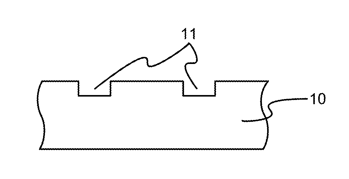
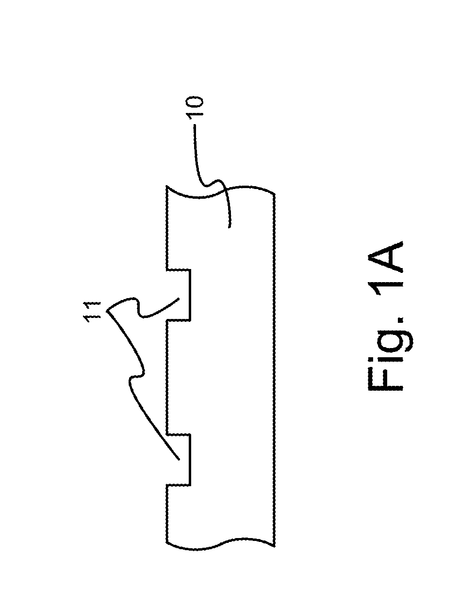
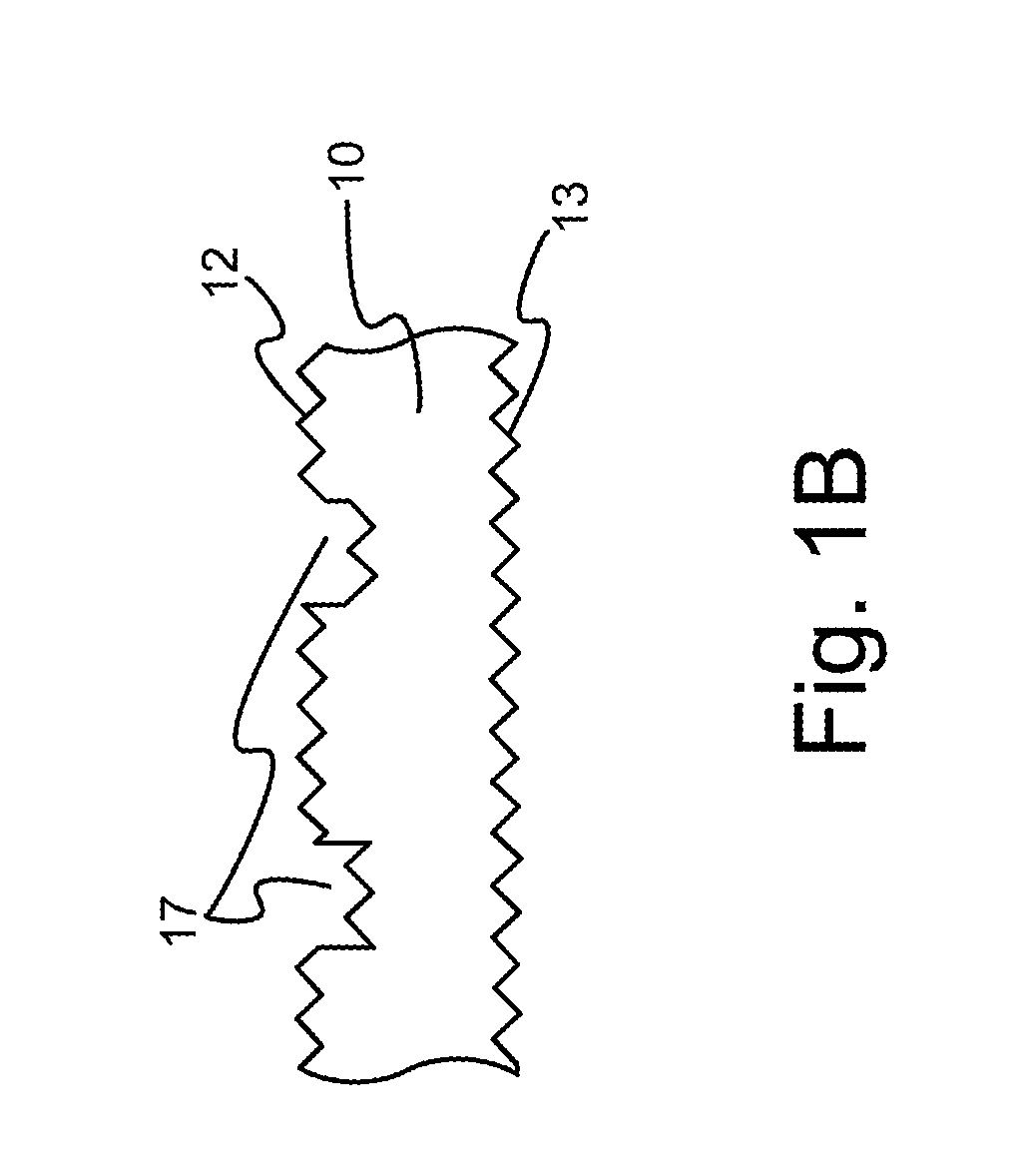
[0017]The present invention is a solar cell having a selective emitter, which is made of a mono-crystalline or multi-crystalline doped silicon substrate. At first, a plurality of trenches are formed on a front surface of the doped silicon substrate, where the trenches have depths between 0.5 micrometers (μm) and 100 μm. Then, the front surface is textured, followed by a diffusion process. The diffusion process produces a heavily-doped layer with a doping polarity opposite to that of the silicon substrate at the near-surface region of the trenches and the near-surface region outside the trenches. Then, the region outside the trenches is etched to a certain depth inside the silicon substrate to turn the corresponding surface region into a lightly-doped diffusion layer so that a selective emitter having heavy and light concentrations is formed...


PUM


Abstract

The present invention provides a solar cell having a selective emitter structure on a doped silicon substrate. The silicon substrate is mono-crystalline or multi-crystalline. A plurality of trenches are formed at the illuminated side of the silicon substrate. After one-time diffusion doping, the silicon substrate is processed through selective etching. The region outside the trenches obtains a lower doping concentration, while the region of the trenches remains to be highly doped. Thus, a selective emitter structure is formed.

Description

TECHNICAL FIELD OF THE INVENTION [0001]The present invention relates to a solar cell; more particularly, relates to forming a plurality of trenches on a silicon substrate through etching; a P-N junction through one-time electronic doping; and a selective emitter through selective etching.DESCRIPTION OF THE RELATED ARTS[0002]A solar cell uses a p-type solar grade silicon substrate to form a p-n junction through phosphorous diffusion, where the silicon substrate has a resistivity between 1 and 3 Ω-cm and a sheet resistance of about 60 Ω / sq after forming the p-n junction. The sheet resistance is obtained at a preferred value through specific adjustment. If the doping concentration for an n-type layer is too high after the diffusion, the sheet resistance will be small. Although it means that the conductivity of the n-type layer is very high and the contact resistance between the front contact and the semiconductor is very low, the recombination rate of carriers at the near-surface regio...

Claims


Application Information

Patent Timeline
Patent Type & Authority Applications(United States)
IPC IPC(8): H01L31/18
CPCH01L31/18H01L31/022425H01L31/068H01L31/1804Y02E10/547Y02P70/50
Inventor WANG, LI-KARN
Owner NATIONAL TSING HUA UNIVERSITY
Why Eureka
Try Eureka