Structure for growth of nitride semiconductor layer, stacked structure, nitride-based semiconductor element, light source, and manufacturing method for same

a technology of nitride-based semiconductors and semiconductor layers, which is applied in the direction of polycrystalline material growth, crystal growth process, chemically reactive gases, etc., can solve the problems of increasing power dissipation, reducing luminous efficacy, and high cost of gan bulk substrates used for crystal growth of nitride-based semiconductor devices whose principal surface is the m-plane. cost, cost reduction

Inactive Publication Date: 2014-03-20
PANASONIC INTELLECTUAL PROPERTY MANAGEMENT CO LTD
View PDF1 Cites 22 Cited by
  • Summary
  • Abstract
  • Description
  • Claims
  • Application Information

AI Technical Summary

Benefits of technology

[0022]In the above-described conventional techniques, further cost reduction and improved quality for formation of the m-plane nitride semiconductor layer have been deman

Problems solved by technology

In the case of an LED, the power dissipation increases, and the luminous efficacy decreases.
However, this GaN bulk substrate which is presently used for crystal growth of a nitride-based semiconductor device of which principal surface is the m-plane is expensive as compared with a sapphire substrate which has been conventionally used for a c-plane GaN-based LED, and also, it is difficult to realize a large diameter.
As for its size, a substrate of m-plane GaN has a square size of about 1-2 cm on each side, and even in the case of a bulk substrate of c-plane GaN, a large diameter of two inches or more is difficult to realize as of now.
This is mainly attributed to a large lattice

Method used


Image

  • Structure for growth of nitride semiconductor layer, stacked structure, nitride-based semiconductor element, light source, and manufacturing method for same
  • Structure for growth of nitride semiconductor layer, stacked structure, nitride-based semiconductor element, light source, and manufacturing method for same
  • Structure for growth of nitride semiconductor layer, stacked structure, nitride-based semiconductor element, light source, and manufacturing method for same

Examples


embodiment 1

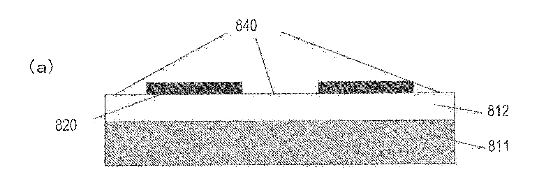
[0189]FIGS. 5(a) and 5(b) are a cross-sectional view and plan view showing a structure for growth of a nitride semiconductor layer (unevenly-processed substrate 910) according to exemplary Embodiment 1.

[0190]As shown in FIG. 5(a), the unevenly-processed substrate 910 includes a sapphire substrate 811 which has an m-plane as a growing plane 811a and a plurality of ridge-shaped nitride semiconductor layers 830 provided on the growing plane 811a of the sapphire substrate 811. Between respective ones of the plurality of ridge-shaped nitride semiconductor layers 830, there are recessed portions 850. In the example shown in FIG. 5(b), the ridge-shaped nitride semiconductor layers 830 extend in a direction which is inclined by angle θ with respect to the c-axis direction of the sapphire substrate 811. Note that, however, in the present embodiment, the extending direction of the ridge-shaped nitride semiconductor layers 830 is not necessarily inclined with respect to the c-axis direction of...

embodiment 2

[0210]Next, a nitride semiconductor growing method of exemplary Embodiment 2 is described with reference to FIG. 9. According to this method, the unevenly-processed substrate 910 of Embodiment 1 and the nitride semiconductor layer which is grown using the unevenly-processed substrate 910 can be formed.

[0211][Preparation of Sapphire Substrate and Preparation of Seed Crystal Nitride Semiconductor Film 812]

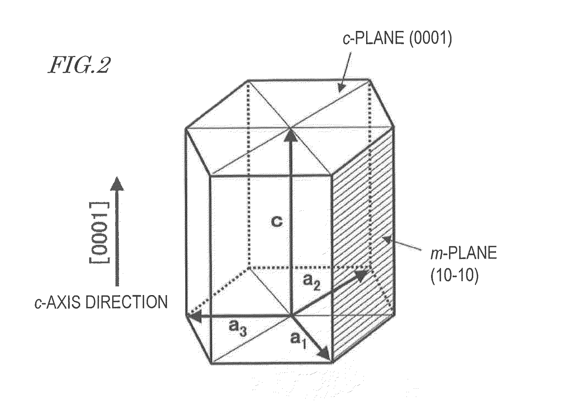
[0212]According to the nitride semiconductor growing method of Embodiment 2, firstly, as shown in FIG. 9(a), an m-plane sapphire substrate 811 is provided. The sapphire substrate 811 used may have a size of 1 inch to 8 inches in diameter, for example. The thickness of the sapphire substrate 811 is, for example, from 0.1 mm to 1 mm. Also, an m-plane sapphire substrate of which substrate surface has an tilt angle (hereinafter, referred to as “off-angle”) may be suitably used. So long as the off-angle is in the range of 0° to 5°, an embodiment of the present disclosure can be carried ou...

##ventive example 1

Inventive Example 1

[0276]Hereinafter, a method for manufacturing a high quality m-plane heterogeneous GaN substrate of the present disclosure is described based on a specific example.

[0277]However, embodiments of the present disclosure are not limited to examples which will be described below.

[0278][Growth of an m-Plane Nitride Semiconductor on an m-Plane Sapphire Substrate that Serves as the Seed Crystal]

[0279]Firstly, a method for manufacturing an m-plane nitride semiconductor on an m-plane sapphire substrate that is used as the seed crystal of this example is described. This manufacturing method includes the following steps:[0280](1) Surface treatment on the m-plane sapphire substrate;[0281](2) Thermal cleaning on the m-plane sapphire substrate;[0282](3) Trimethyl aluminum (TMA) source material irradiation on the m-plane sapphire substrate and low temperature AlxGayInzN (0≦x, y, z≦1, x+y+z=1) buffer layer growth; and[0283](4) Growth of an m-plane GaN film.

Hereinafter, the respect...


PUM


Abstract

A structure for growth of a nitride semiconductor layer which is disclosed in this application includes: a sapphire substrate of which growing plane is an m-plane; and a plurality of ridge-shaped nitride semiconductor layers provided on the growing plane of the sapphire substrate, wherein a bottom surface of a recessed portion provided between respective ones of the plurality of ridge-shaped nitride semiconductor layers is the m-plane of the sapphire substrate, the growing plane of the plurality of ridge-shaped nitride semiconductor layers is an m-plane, and an absolute value of an angle between an extending direction of the plurality of ridge-shaped nitride semiconductor layers and a c-axis of the sapphire substrate is not less than 0° and not more than 35°.

Description

[0001]This is a continuation of International Application No. PCT / JP2012 / 004958, with an international filing date of Aug. 3, 2012, which claims priority of Japanese Patent Applications No. 2011-174300, filed on Aug. 9, 2011, No. 2011-257924, filed on Nov. 25, 2011, and No. 2012-019641, filed on Feb. 1, 2012, the contents of which are hereby incorporated by reference.BACKGROUND[0002]1. Technical Field[0003]The present disclosure relates to a structure for growth of a nitride semiconductor layer, a multilayer structure including that structure, a nitride-based semiconductor device including that multilayer structure, and a light source including that nitride-based semiconductor device, and manufacturing methods thereof.[0004]2. Description of the Related Art[0005]A nitride semiconductor containing nitrogen (N) as a Group V element is a prime candidate for a material to make a short-wave light-emitting device because its bandgap is sufficiently wide. Among other things, gallium nitrid...

Claims


Application Information

Patent Timeline
IPC IPC(8): H01L33/32H01L21/20
CPCH01L21/20H01L33/32C30B25/04C30B25/18H01L33/16H01L21/0242H01L21/0243H01L21/02433H01L21/02458H01L21/0254H01L21/02639H01L21/0265H01L33/007H01L33/20C30B29/403H01L33/12H01L21/0262H01L21/02609H01L21/02642H01L2224/16225H01L2224/14H01L33/18H01L33/58
Inventor CHOE, SONGBAEKYOKOGAWA, TOSHIYAINOUE, AKIRAYAMADA, ATSUSHI
Owner PANASONIC INTELLECTUAL PROPERTY MANAGEMENT CO LTD
Why Eureka
Try Eureka