Semiconductor device

a technology of semiconductor devices and semiconductors, applied in semiconductor devices, diodes, electrical devices, etc., can solve the problem of disadvantageous expansion of the termination structure region

Active Publication Date: 2014-03-20
MITSUBISHI ELECTRIC CORP
View PDF2 Cites 3 Cited by
  • Summary
  • Abstract
  • Description
  • Claims
  • Application Information

AI Technical Summary

Benefits of technology

[0011]Regarding the semiconductor device of the present invention, a breakdown voltage can sufficiently be ensured without expansion of the electric-field reduction region provided as the termination structure portion.

Problems solved by technology

The conventional semiconductor device, however, has the following problem.
Specifically, because the semiconductor device has, in the termination structure portion, an insulator region formed between a guard ring region and a channel stopper region, the region of the termination structure portion is disadvantageously expanded.

Method used


Image

  • Semiconductor device
  • Semiconductor device
  • Semiconductor device

Examples


first embodiment

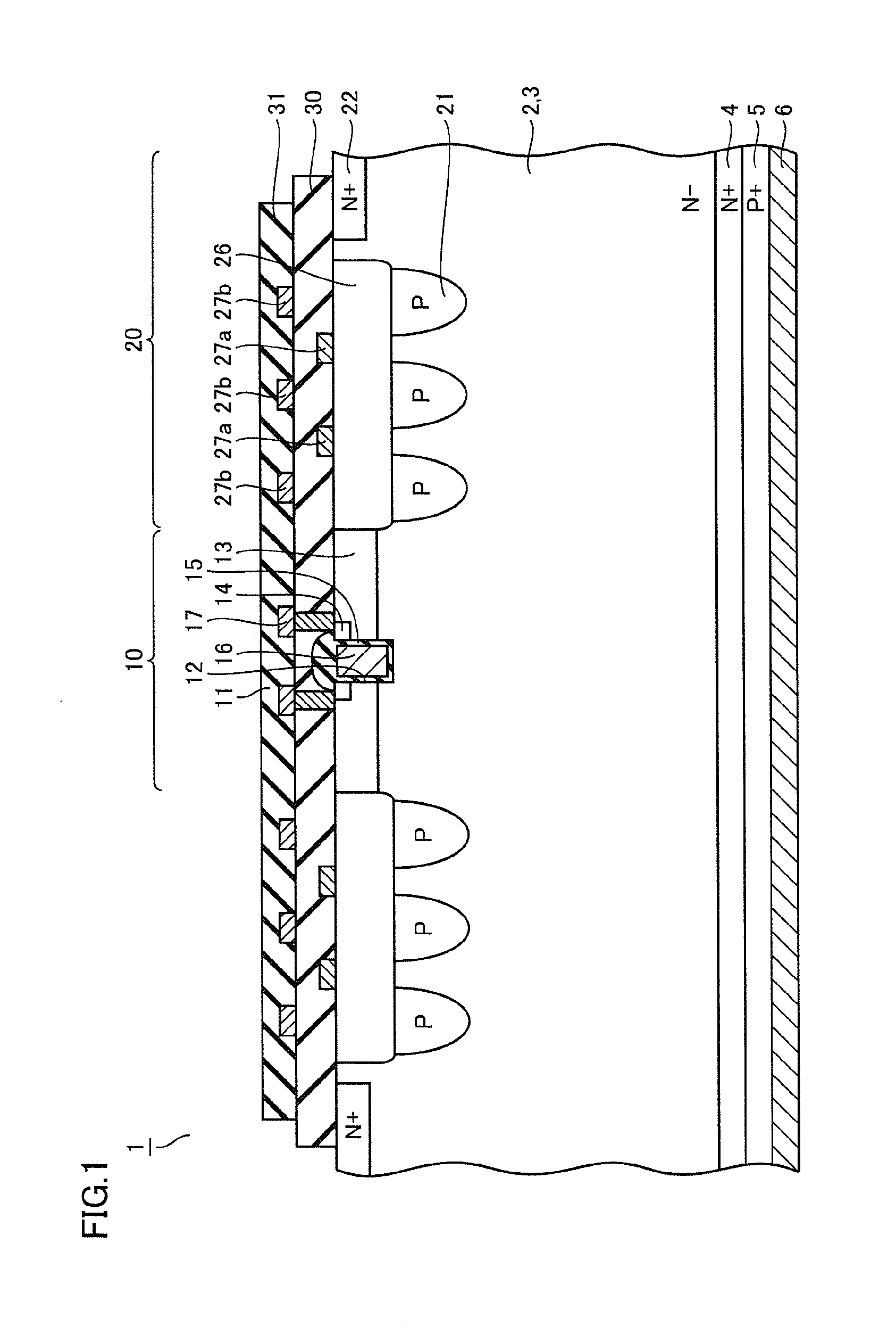
[0031]A semiconductor device in a first embodiment of the present invention will be described. As shown in FIG. 1, semiconductor device 1 includes an n− layer 3 formed from one surface of a semiconductor substrate 2 to a predetermined depth. In a predetermined region of n− layer 3, an active region 10 in which main current flows is formed. Active region 10 serves as an element-formed region. In active region 10, an IGBT 11 is formed as an example of switching elements.

[0032]In active region 10, a p base layer 13 is formed. A trench 12 is formed from the surface of p base layer 13 to extend through p base layer 13 and reach n− layer 3. In trench 12, a gate buried electrode 16 is formed so that a gate oxide film 15 on the side wall of trench 12 is interposed between the trench and the electrode. From the surface of p base layer 13 to a predetermined depth, an n+ emitter layer 14 is also formed. FIG. 1 shows, for the sake of simplification of the drawing, one IGBT 11 formed in active r...

third modification

[0069]A third modification of the semiconductor device in the first embodiment, specifically another semiconductor device having a trench structure in the termination structure portion will be described.

[0070]As shown in FIG. 11, semiconductor device 1 includes a plurality of trenches 28 formed through a porous-oxide-film region 26. These trenches 28 are spaced from each other along the direction connecting active region 10 and channel stopper region 22. A guard ring region 21 serving as a breakdown voltage layer is formed to surround the lateral and lower sides of a portion of trench 28 that extends downward from porous-oxide-film region 26.

[0071]A floating electrode 27a is formed in a bottom portion of trench 28. A floating electrode 27b is also formed on the surface of porous-oxide-film region 26 that is located in the vicinity of the opening end of trench 28. A first insulating film 30 is formed to fill trenches 28. Features other than the above-described ones are similar to tho...

second embodiment

[0077]A semiconductor device in a second embodiment of the present invention will be described. As shown in FIG. 13, semiconductor device 1 includes a porous-oxide-film region 26 formed in a stepwise manner to extend gradually deeper from a side of p base layer 13 toward a side of channel stopper region 22. Features other than the above-described ones are similar to those of the semiconductor device shown in FIG. 1. Therefore, the same components are denoted by the same reference characters, and the description thereof will not be repeated.

[0078]In the following, operations will briefly be described. Regarding an ON operation, a predetermined voltage equal to or higher than a threshold voltage is applied to gate buried electrode 16 to thereby cause the MOS channel to be rendered ON, cause electrons and holes to be injected into n− layer 3, and accordingly cause a conductivity modulation, which reduces the voltage between collector electrode 6 and emitter electrode 17 and causes an O...


PUM

PropertyMeasurementUnit
conductivity typeaaaaaaaaaa
electric-fieldaaaaaaaaaa
dielectric constantaaaaaaaaaa

Abstract

In one surface of a semiconductor substrate, an active region in which main current flows and an IGBT is disposed is formed. A termination structure portion serving as an electric-field reduction region is formed laterally with respect to the active region. In the termination structure portion, a porous-oxide-film region, a p-type guard ring region, and an n+-type channel stopper region are formed. A plurality of floating electrodes are formed to contact the surface of the porous-oxide-film region. Another plurality of floating electrodes are formed to contact a first insulating film.

Description

BACKGROUND OF THE INVENTION[0001]1. Field of the Invention[0002]The present invention relates to a semiconductor device, and particularly to a power semiconductor device.[0003]2. Description of the Background Art[0004]A vertical-type semiconductor device is a type of power semiconductor device. In the vertical-type semiconductor device, electric current is conducted (ON state) or interrupted (OFF state) between a front surface side and a rear surface side of the semiconductor device. On the front surface side of the semiconductor substrate, for example, a region is formed in which a switching element such as IGBT (Insulated Gate Bipolar Transistor) and the like are arranged. In this region, main current flows when the semiconductor device is electrically conductive, and this region is called active region.[0005]In the case where the semiconductor device is a power device for which a high breakdown voltage is required, the front surface side of a semiconductor substrate includes the ...

Claims


Application Information

Patent Timeline
Patent Type & Authority Applications(United States)
IPC IPC(8): H01L27/06
CPCH01L27/0629H01L29/7397H01L29/0623H01L29/063H01L29/404H01L29/407H01L29/0619H01L29/7803H01L29/7811H01L29/7813H01L29/0615H01L29/0638H01L29/0649H01L29/0653H01L29/1095
Inventor AKIYAMA, HAJIMEOKADA, AKIRA
Owner MITSUBISHI ELECTRIC CORP
Why Eureka
Try Eureka