Die cap for use with flip chip package

a technology of flip chip and die cap, which is applied in the direction of semiconductor devices, semiconductor/solid-state device details, electrical devices, etc., can solve the problems of stress-caused failure, large warpage, and increased stress level inside flip chip packages, so as to reduce the risk of the die cap delaminate from the die. , the effect of improving thermal performan

Inactive Publication Date: 2014-04-03
SHEN YUCI
View PDF9 Cites 70 Cited by
  • Summary
  • Abstract
  • Description
  • Claims
  • Application Information

AI Technical Summary

Benefits of technology

[0013]In one embodiment of the present invention, a die cap comprises a top piece, four side walls with or without a foot edge on the bottom of each side wall and some specific elements including 1) an edge notch on the inner surface and along the edge of the top piece of the die cap (referred to as an edge notch herein), 2) some bumps on the middle part of the inner surface of the top piece (referred to as middle bumps herein), 3) a top edge extending outwards from the top piece (referred to as a top edge herein), 4) side support walls or side support posts extending downwards from the top edge of the top piece (referred to as side support walls or side support posts herein). The terminologies of edge notch, middle bumps, top edge, side support walls and side support posts involved in the die cap of the present invention and the foot edge in the convention lid will be explained further with reference to their drawings below. Besides the major purpose of the die cap to control the warpage of the flip chip packages, these specific elements of the die cap of the present invention can improve the thermal performance and reduce the risk for the die cap to delaminate from the die.
[0016]The conventional method for reducing the warpage of flip chip packages is to constrain the thermal deformation of the substrate of flip chip packages by attaching a lid or a die clip on the substrate in prior arts. The inventive concept of present invention for reducing the warpage of flip chip packages is to directly constrain the thermal deformation of the die by bonding a die cap around the die of flip chip packages. The spirit of the present invention can be easily extended for reducing the warpage and improving the reliability of other semiconductor packages. For example, a die cap can cover an assembly of multiple stack dice to form a capped assembly of multiple stack dice. Accordingly, the warpage of flip chip packages using a capped assembly of multiple stack dice is reduced. More features and advantages of the present invention are described with reference to the detailed description of the embodiments of the present invention below.

Problems solved by technology

A large warpage is a big issue for flip chip packages using an organic substrate, especially for flip chip packages with a big substrate size and big die size.
When using the conventional stiffener or lid to reduce the warpage of flip chip packages, the stress level inside flip chip packages is usually increased as a trade-off, leading to some stress-caused failure issues.
The big CTE mismatch between the die and substrate is the root cause for such issues of the flip chip package as large warpage, dielectric layer cracking, bump bridging and bump cracking in its manufacture, application or reliability test.
A disadvantage of such an application of lids in flip chip packages is that there is a cavity between the die sides and the lid.
As a result, the sides of the die 32 are not constrained effectively by the lids, giving a low efficiency for reducing the warpage of flip chip packages.
A disadvantage of the prior arts illustrated in FIG. 3 and FIG. 4 is that the die clip or one piece of the multi-piece heat spreader is attached with the substrate prior to the dispensation of the underfill material into the gap between the die and the substrate.
As a result, one or more openings on the side portion of the die clip or the multi-piece heat spreader is needed, leading to a complicated assembly process of a flip chip package using the die clip or multi-piece heat spreader.
Furthermore, when mounting a flip chip package with the die cap on a board or PCB for its field application, the board level reliability of the flip chip package is improved as well because the CTE mismatch is also the root cause for the reliability issue of the solder balls between the substrate and the board or PCB.

Method used


Image

  • Die cap for use with flip chip package
  • Die cap for use with flip chip package
  • Die cap for use with flip chip package

Examples


Embodiment Construction

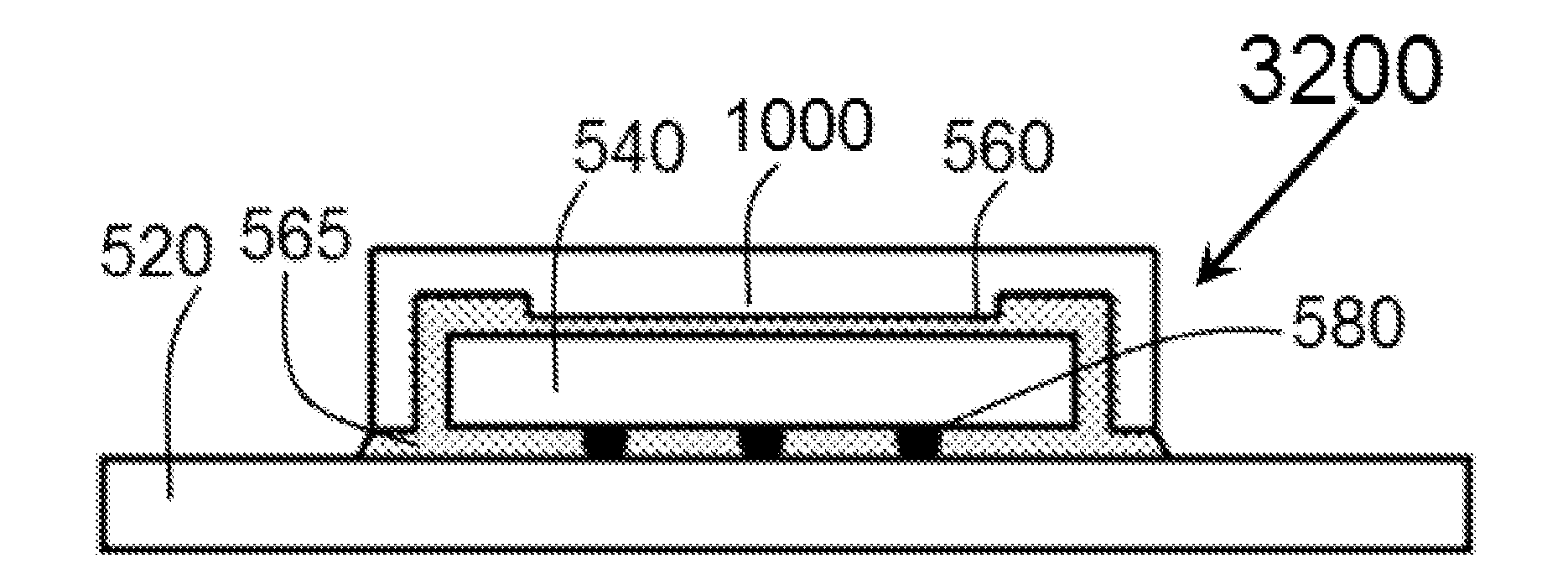
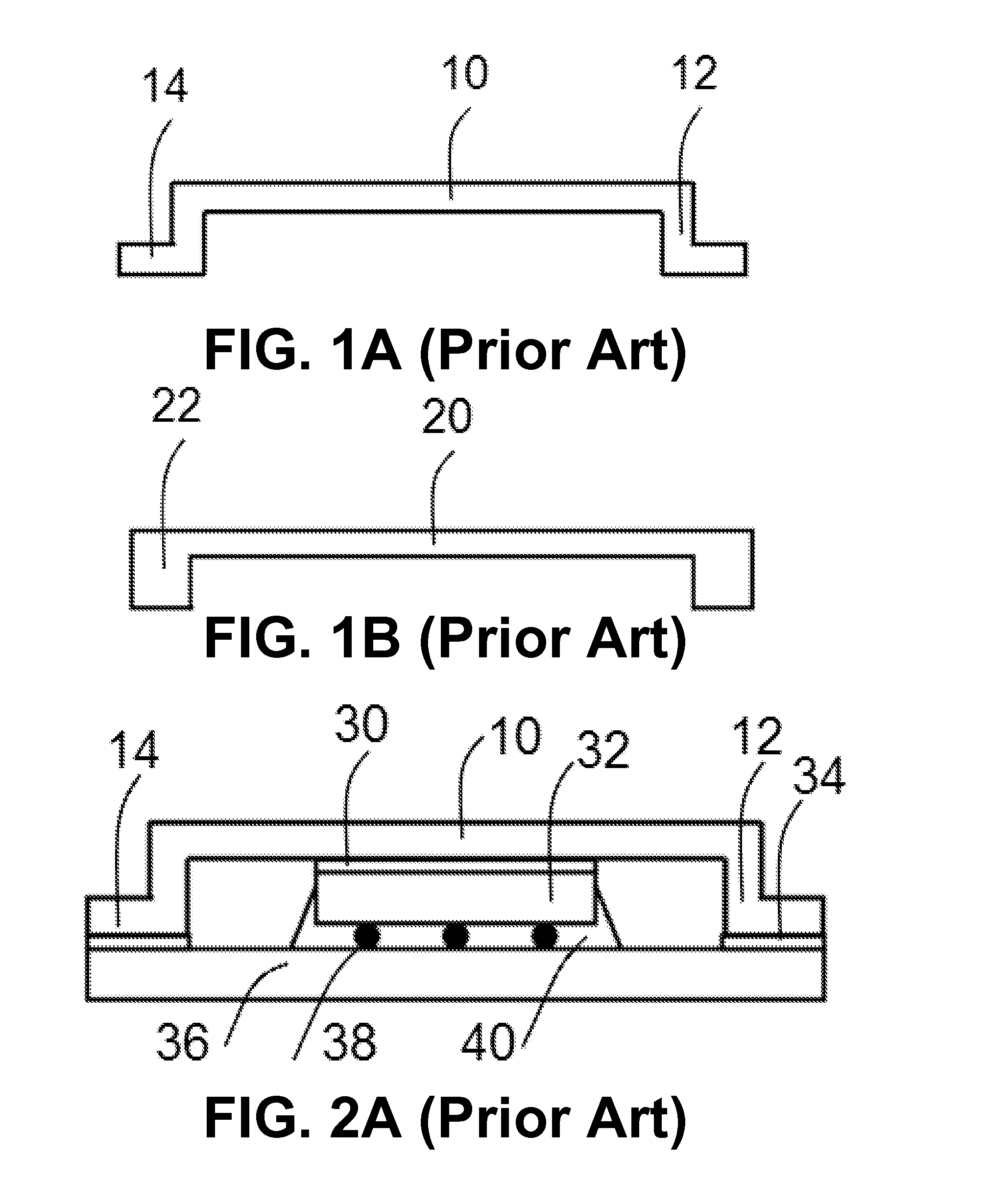
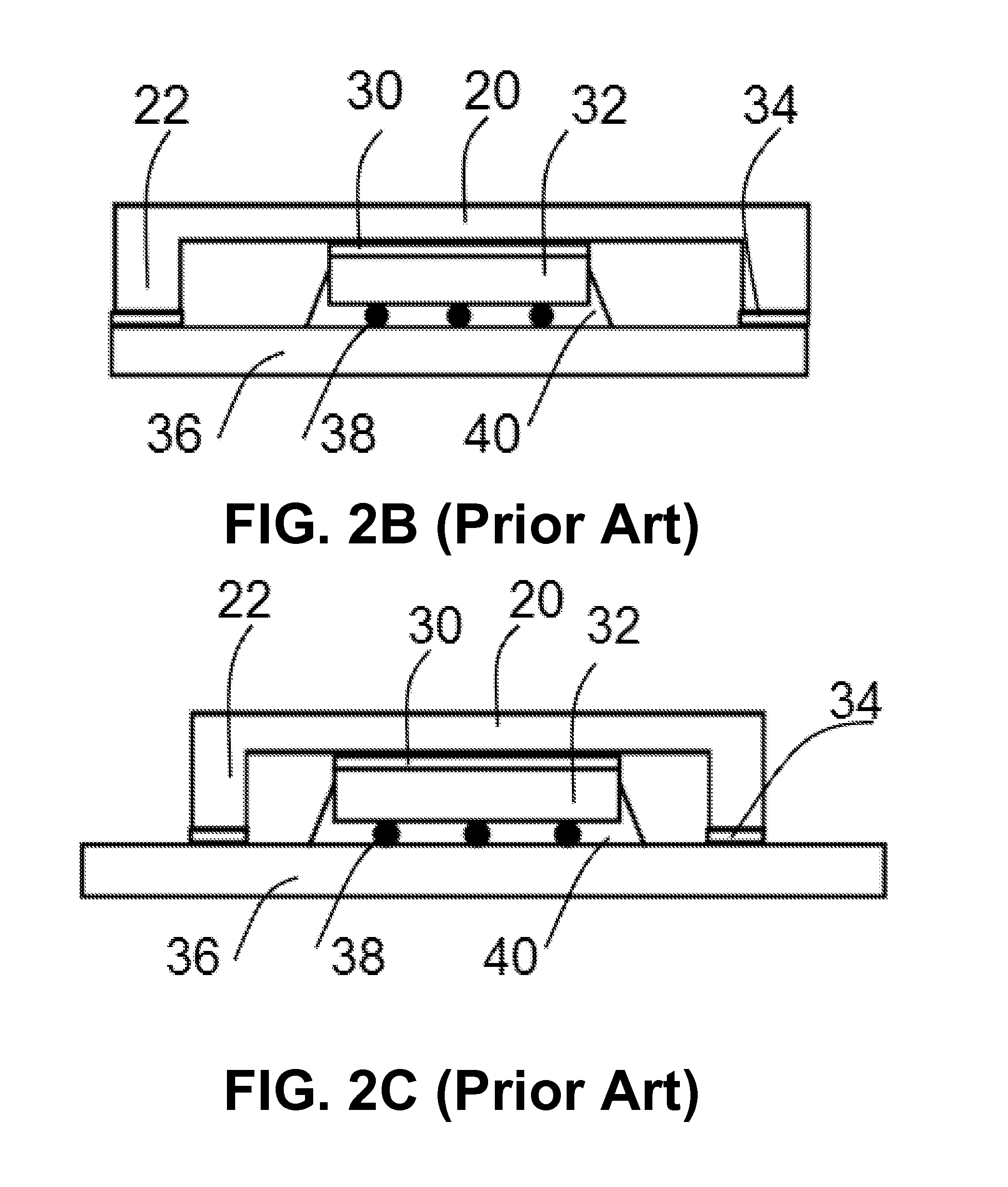
[0030]Referring to FIG. 5A, a schematic cross-sectional diagram of a die cap 1000 is shown, wherein the die cap comprises a top piece 100, side walls 120 and an edge notch 140 on the inner surface and along the edge of the top piece 100. The purpose of the edge notch 140 is to make the thickness of adhesive layer between a die and the die cap thick and thin on the outer and inner parts separately when covering the die cap on the die. As a result, the risk of delamination failure between the die and die cap may be reduced without significantly affecting thermal dissipation capability from die to die cap. Referring to FIG. 5B, a schematic cross-sectional diagram of a die cap 1200 is showed, wherein the die cap comprises a top piece 100, four side walls 120, an edge notch 140 along the edge of top piece and a foot edge 160 at the bottom of each side wall. The die caps 1000 and 1200 showed in FIGS. 5A and 5B have an edge notch 140, which is the first specific feature of the die cap of o...


PUM


Abstract

A die cap for use with flip chip packages, flip chip packages using a die cap, and a method for manufacturing flip chip packages with a die cap are provided in the invention. A die cap encases the die of flip chip packages about its top and sides for constraining the thermal deformation of the die during temperature change. The CTE (coefficient of thermal expansion) mismatch between the die and substrate of flip chip packages is the root cause for warpage and reliability issues. The current inventive concept is to reduce the CTE mismatch by using a die cap to constrain the thermal deformation of the die. When a die cap with high CTE and high modulus is used, the die with the die cap has a relatively high overall CTE, reducing the CTE mismatch. As a result, the warpage and reliability of flip chip packages are improved.

Description

TECHNICAL FIELD OF THE INVENTION[0001]The present invention generally relates to integrated circuit semiconductor packages. The present invention particularly relates to a die cap and its application for reducing the warpage and improving the reliability of flip chip semiconductor packages.BACKGROUND OF THE INVENTION[0002]Flip Chip interconnect technology is extensively used for packaging semiconductor devices because of its capability for accommodating very high pin count per area. The very common semiconductor packages using flip chip interconnect technology includes flip chip packages. A flip chip package primarily comprises a die and a substrate, wherein the die with electrically conductive bumps such as solder bumps or cu pillar solder bumps on its active surface is attached on one side of the substrate. An underfill material is usually dispensed into the gap between the die and the substrate through a capillary force to protect solder bumps. Flip chip packages include flip chi...

Claims


Application Information

Patent Timeline
Patent Type & Authority Applications(United States)
IPC IPC(8): H01L23/498H01L21/50
CPCH01L25/0655H01L2224/16225H01L2224/32225H01L2224/32245H01L2224/73204H01L2224/73253H01L2224/92125H01L2225/1023H01L2225/1058H01L2924/15311H01L2924/15331H01L2924/3511H01L23/24H01L23/3107H01L21/563H01L2924/16251H01L2924/1615H01L2924/16153H01L2924/00012H01L2924/00
Inventor SHEN, YUCI
Owner SHEN YUCI
Why Eureka
Try Eureka