

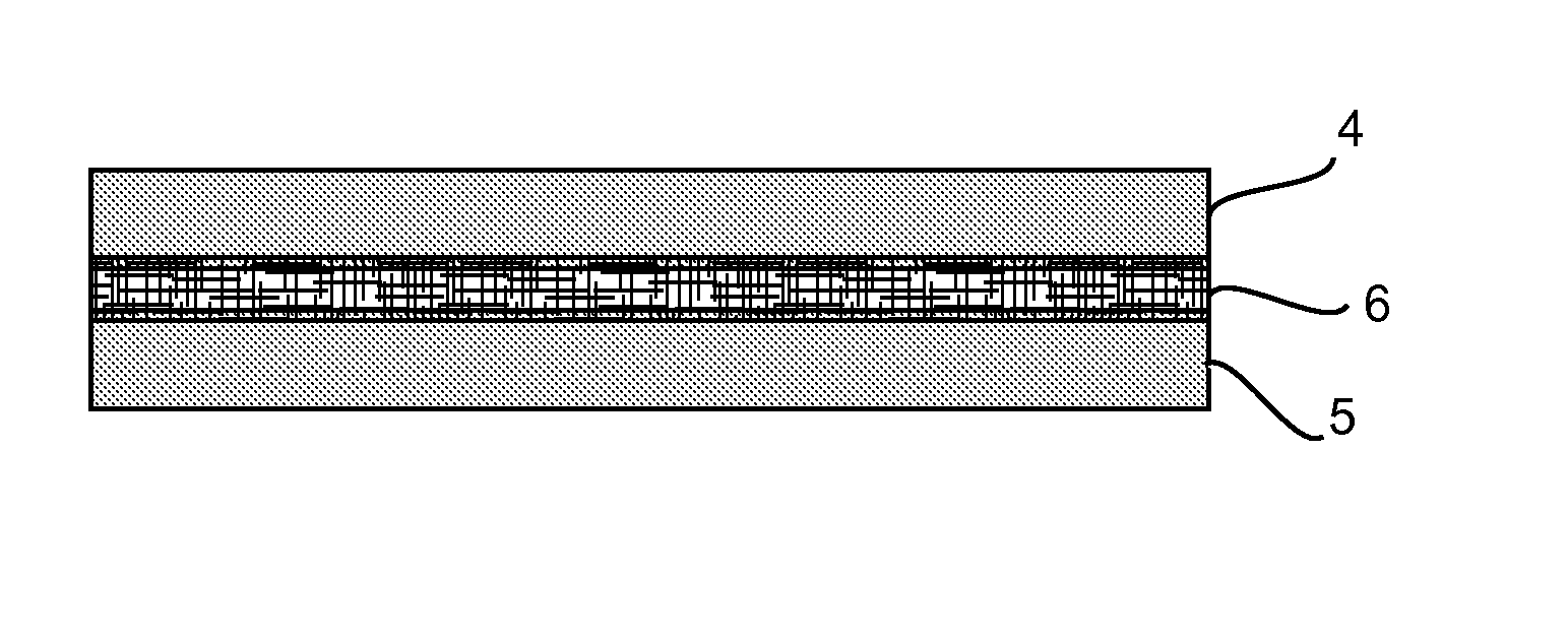
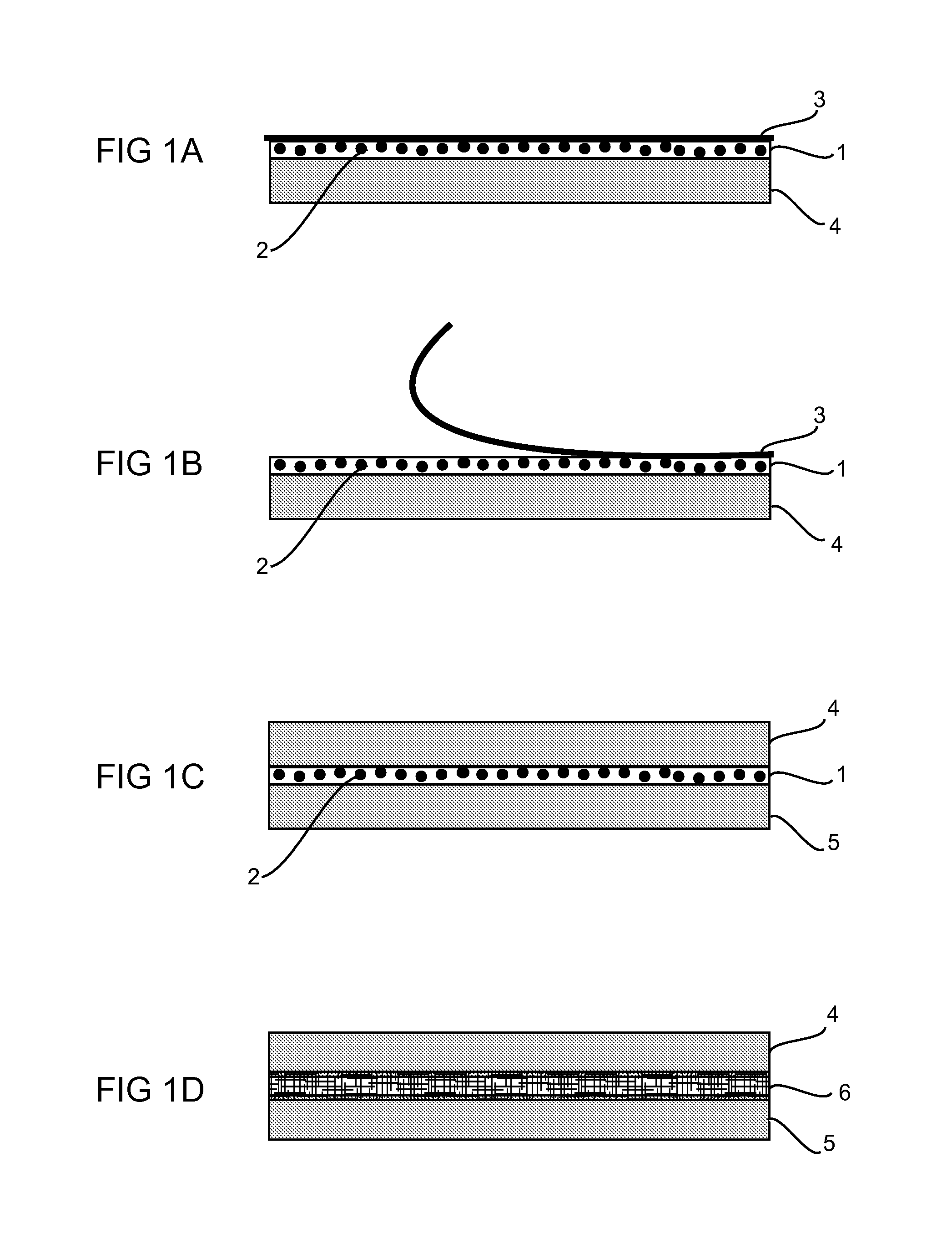
Conductive film adhesive
a technology of conductive film and adhesive, which is applied in the field of adhesives, can solve the problems of affecting the performance of the solder bonding process, the deterioration of the electrical and thermal conductivity reliant on particle-to-particle and particle-to-adherent contact, and the insufficient thermal conductivity, which is a function of the contact area,
- Summary
- Abstract
- Description
- Claims
- Application Information
AI Technical Summary
Benefits of technology
Problems solved by technology
Method used
Image

Examples
example 1
TLPS Films Containing 41% Copper / 50% Tin Bismuth Alloy
[0087]A varnish was prepared by combing the following components in the amounts indicated below in Table 1 with cyclopentanone solvent in a jar and mixing by hand with a metal spatula.
TABLE 1Composition of 41% Copper / 50% SnBi Alloy VarnishComponent typeSpecific ComponentWeight %FluxGlutaric acid0.16(carboxylic acid +N,N,N′,N′ tetrakis(2-hydroxyethyl)0.84tertiary amine)ethylenediamineThermosettingEpoxy HP-7200L3.35resin (1)(DIC Corporation)ThermosettingEpoxy jER828EL1.75resin (2)(Mitsubishi Chemical Corporation)Curing agentImidazole 2PHZ-PW0.20(Shikoku Chemicals Corporation)PolymerPhenoxy YP-50S2.7(Nippon Steel Chemical Corporation)Metal filler (1)Cu (elemental) spherical41.0(Metal filler (2)SnBi (80:20 wt. %) spherical50.0(Total100
[0088]The varnish mixture then underwent a second mixing using a high shear disperser to help the solid blend components with the liquid components. After the high shear dispersing mix, the varnish mixt...
example 2
TLPS Films Containing 60% Copper / 31% Tin Bismuth Alloy
[0089]A varnish was prepared by combing the following components in the amounts indicated below in Table 2 with cyclopentanone solvent in a jar and mixing by hand with a metal spatula.
TABLE 2Composition of 60% Copper / 31% SnBi Alloy VarnishComponent typeSpecific ComponentWeight %FluxOxalic acid0.16(Carboxylic acid +N,N,N′,N′ tetrakis(2-hydroxyethyl)0.84Tertiary amine)ethylenediamineThermosettingEpoxy HP-7200L3.35resin (1)(DIC Corporation)ThermosettingEpoxy jER828EL1.75resin (2)(Mitsubishi Chemical Corporation)Curing agentImidazole 2PHZ-PW0.20(Shikoku Chemicals Corporation)PolymerPhenoxy YP-50S2.7(Nippon Steel Chemical Corporation)Metal filler (1)Cu (elemental) spherical60(Metal filler (2)SnBi (80:20 wt. %) spherical31(Total100
[0090]The varnish mixture then underwent a second mixing using a high shear disperser to help blend the solid components with the liquid components. After the high shear dispersing mix, the varnish mixture wa...
example 3
TLPS Film Containing 65% Copper / 26% SnBi Alloy
[0091]A varnish was prepared by combing the following components in the amounts indicated below in Table 3 with cyclopentanone solvent in a jar and mixing by hand with a metal spatula.
TABLE 3Compositions of 65% Copper / 26% SnBi Alloy VarnishComponent typeSpecific ComponentWeight %FluxOxalic acid0.16(Carboxylic acid +N,N,N′,N′ tetrakis(2-hydroxyethyl)0.84Tertiary amine)ethylenediamineThermosettingEpoxy HP-7200L3.35resin (1)(DIC Corporation)ThermosettingEpoxy jER828EL1.75resin (2)(Mitsubishi Chemical Corporation)Curing agentImidazole 2PHZ-PW0.20(Shikoku Chemicals Corporation)PolymerPhenoxy YP-50S2.7(Nippon Steel ChemicalCorporation)Metal filler (1)Cu (elemental) spherical65(Metal filler (2)SnBi (80:20 wt. %) spherical26(Total100
[0092]The varnish mixture then underwent a second mixing using a high shear disperser to help blend the solid components with the liquid components. After the high shear dispersing mix, the varnish mixture was de-aer...
PUM
| Property | Measurement | Unit |
|---|---|---|
| Fraction | aaaaa | aaaaa |
| Percent by mass | aaaaa | aaaaa |
| Percent by mass | aaaaa | aaaaa |
Abstract
Description
Claims
Application Information