
Solution-Processed Metal-Selenide Semiconductor Using Selenium Nanoparticles

a technology of selenium nanoparticles and metal selenide semiconductors, applied in the field of metal selenide semiconductor film formation using selenium nanoparticle solutions, can solve the problems of high toxicity and reactivity associated with hydrazine, selenium loss, and resultant cigs film as selenium deficient, so as to reduce cigs film contamination, and reduce the effect of macromolecular or poly

Inactive Publication Date: 2014-05-15
SHARP KK
View PDF4 Cites 5 Cited by
  • Summary
  • Abstract
  • Description
  • Claims
  • Application Information

AI Technical Summary

Benefits of technology

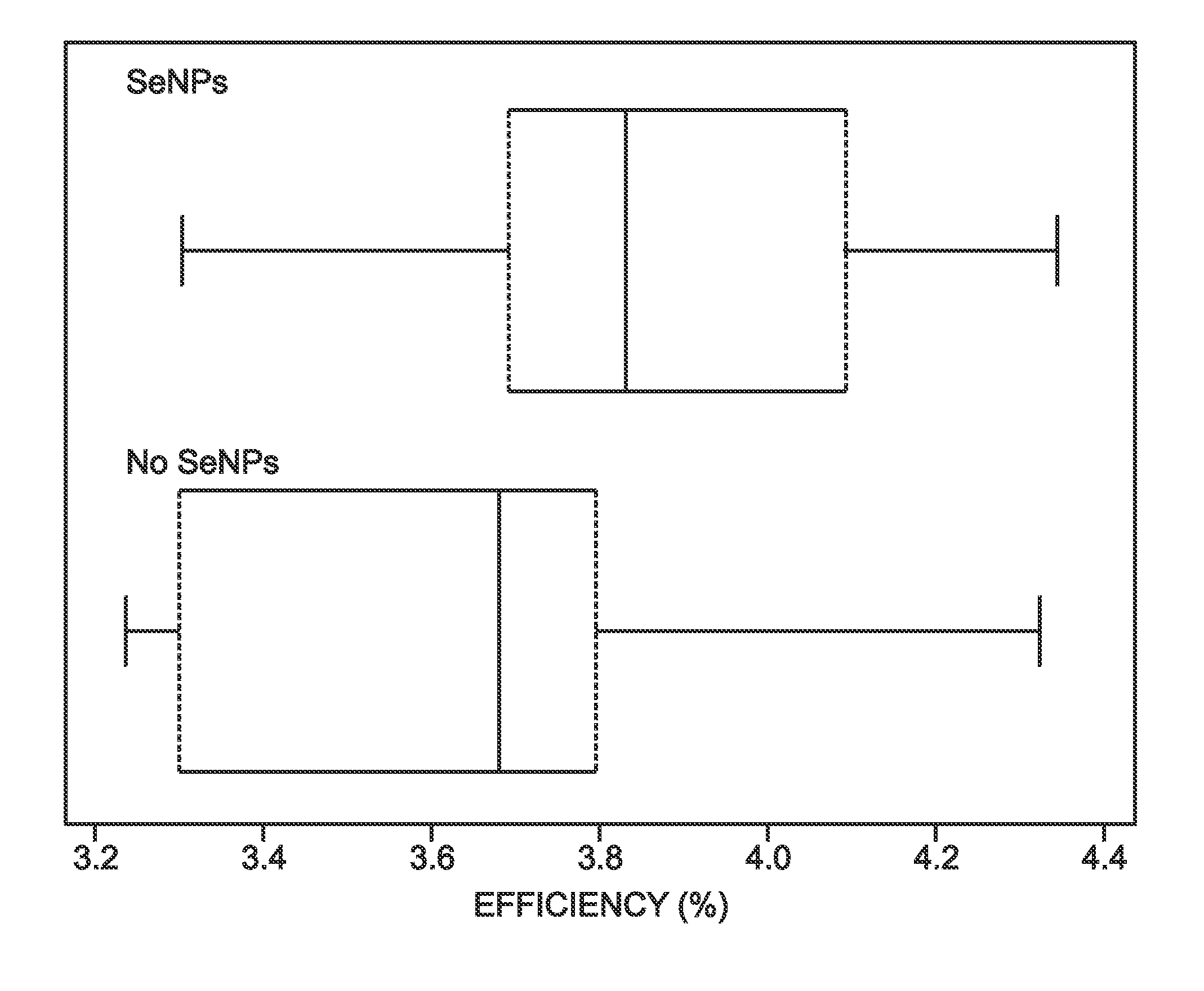
The patent text describes a method for supplying selenium in the form of selenium nanoparticles (SeNPs) for solution-based processing, specifically in the fabrication of a copper indium gallium diselenide (CuIn1-xGaxSe2 or CIGS) absorber layer for photovoltaic (PV) applications. The SeNPs are stabilized in a way that minimizes CIGS film contamination during thermal processing, and are compatible with other components within an established solution-based formulation. The SeNPs must also be small in size (<200 nm) and high in concentration in order to supply sufficient selenium for a beneficial impact on CIGS film formation and quality during thermal processing. The method involves depositing a first solution containing the SeNPs on a conductive substrate, followed by a second solution containing a first material set of metal salts, metal complexes, or combinations thereof, which are dissolved in a solvent. The second solution is deposited on the substrate, forming a first intermediate film comprising metal precursors, made from corresponding members of the first material set, and embedded SeNPs. The first intermediate film is then thermally annealed, resulting in the transformation of the metal precursors and the selenization of the film, forming a first metal selenide-containing semiconductor.

Problems solved by technology

Mitzi et al. described a solution-based CIGS deposition strategy using homogenous solutions of Cu, In, Ga and Se (and optionally sulfur) obtained by dissolution in hydrazine.1 Subsequently, a hydrazine-free approach was reported whereby isolated hydrazinium-based precursors could be deposited to form metal chalcogenide composite films.2 Unfortunately, the high toxicity and reactivity associated with hydrazine is a major disadvantage for these approaches.
Unfortunately, most conventional CIGS fabrication strategies require high temperature post-selenization following deposition of the copper, indium, and gallium (CIG) absorber layer.
Even in those cases where selenium is integrated into the components before or during the film deposition phase (as in Se containing metal selenide nanoparticles or solution based process with Se precursor), selenium losses during high temperature processing can render the resultant CIGS film as selenium deficient.
In addition, an inability for the selenium source vapor to penetrate deep into a deposited CIG film may lead to reduced grain size, poor overall absorber layer growth, and / or morphology as well as poor interfacial contacts.
One of the major disadvantages of high temperature selenization (H2Se gas or Se fluxes, for example) is the inherent high-toxicity, which can present serious hazards to humans in large-scale production environments.
Furthermore, the high-temperature associated with the selenization processes imposes severe limitations on the types of substrates upon which CIGS can be deposited.
Despite the novelty of the approach, there exist limited cases in which SeNPs have been suggested as viable options for a solution processed CIGS absorber layer.
In some ways, this may be explained by the difficulties associated with synthesizing stable dispersions of SeNPs that can be practically utilized in a precursor solution for CIGS deposition.
Unfortunately, the use of SeNPs stabilized by exceptionally large species is impractical due to extensive contamination by carbon, oxygen, and nitrogen species upon thermal decomposition, which prevents the realization of high-quality CIGS films.

Method used


Image

  • Solution-Processed Metal-Selenide Semiconductor Using Selenium Nanoparticles
  • Solution-Processed Metal-Selenide Semiconductor Using Selenium Nanoparticles
  • Solution-Processed Metal-Selenide Semiconductor Using Selenium Nanoparticles

Examples


Embodiment Construction

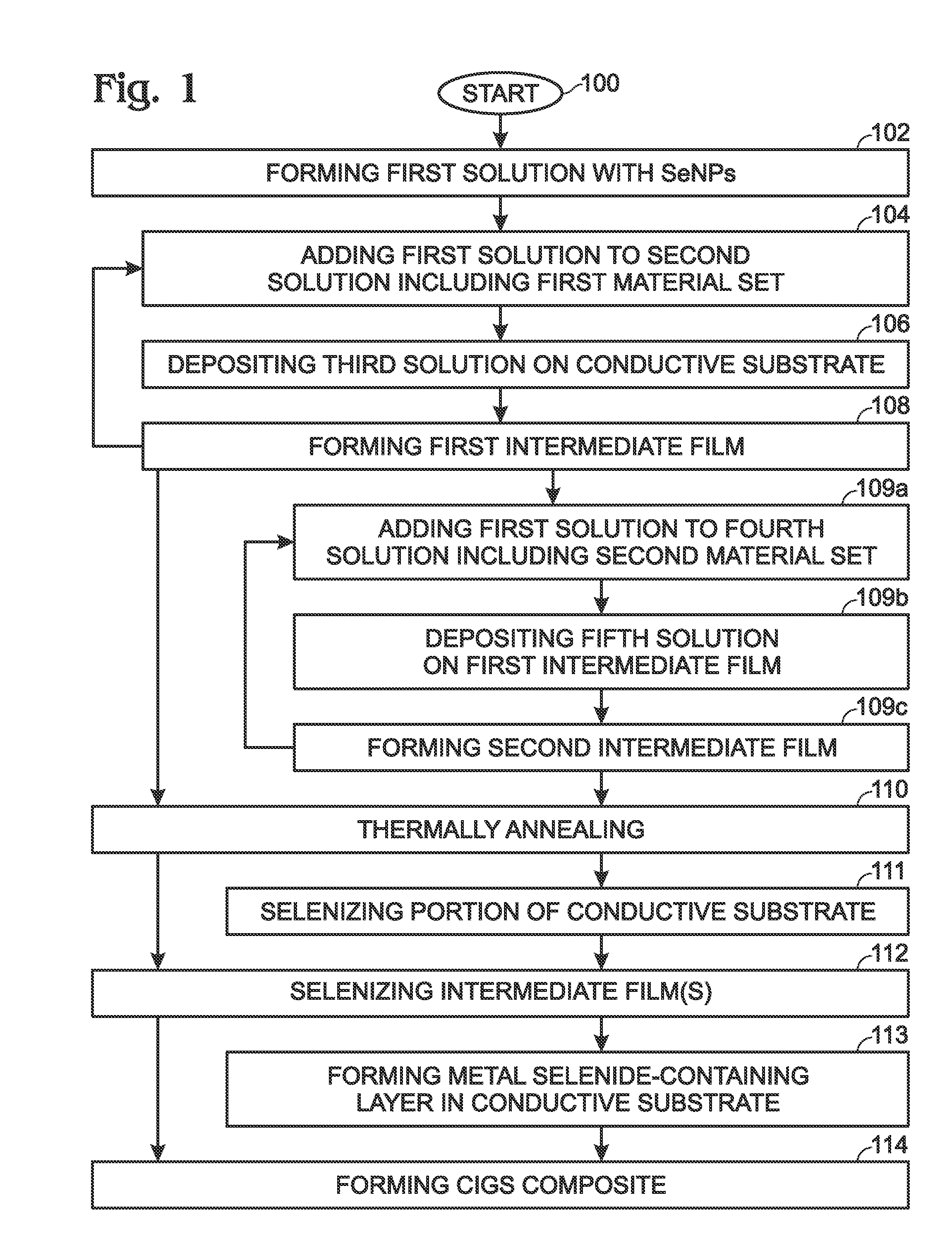
[0035]FIG. 1 is a flowchart illustrating steps in a method for forming a solution-processed copper indium gallium diselenide (CIGS) absorber using selenium (Se) nanoparticles (NPs). Although the method is depicted as a sequence of numbered steps for clarity, the numbering does not necessarily dictate the order of the steps. It should be understood that some of these steps may be skipped, performed in parallel, or performed without the requirement of maintaining a strict order of sequence. Generally however, the method follows the numeric order of the depicted steps. The method begins at Step 100.

[0036]Step 102 forms a first solution including SeNPs dispersed in a solvent. Step 104 adds the first solution to a second solution including a first material set. The first material set may be comprised of metal salts and metal complexes of copper (Cu), indium (In), gallium (Ga), or combinations thereof, dissolved in a solvent. The result is the formation of a third solution. Step 106 depos...


PUM


Abstract

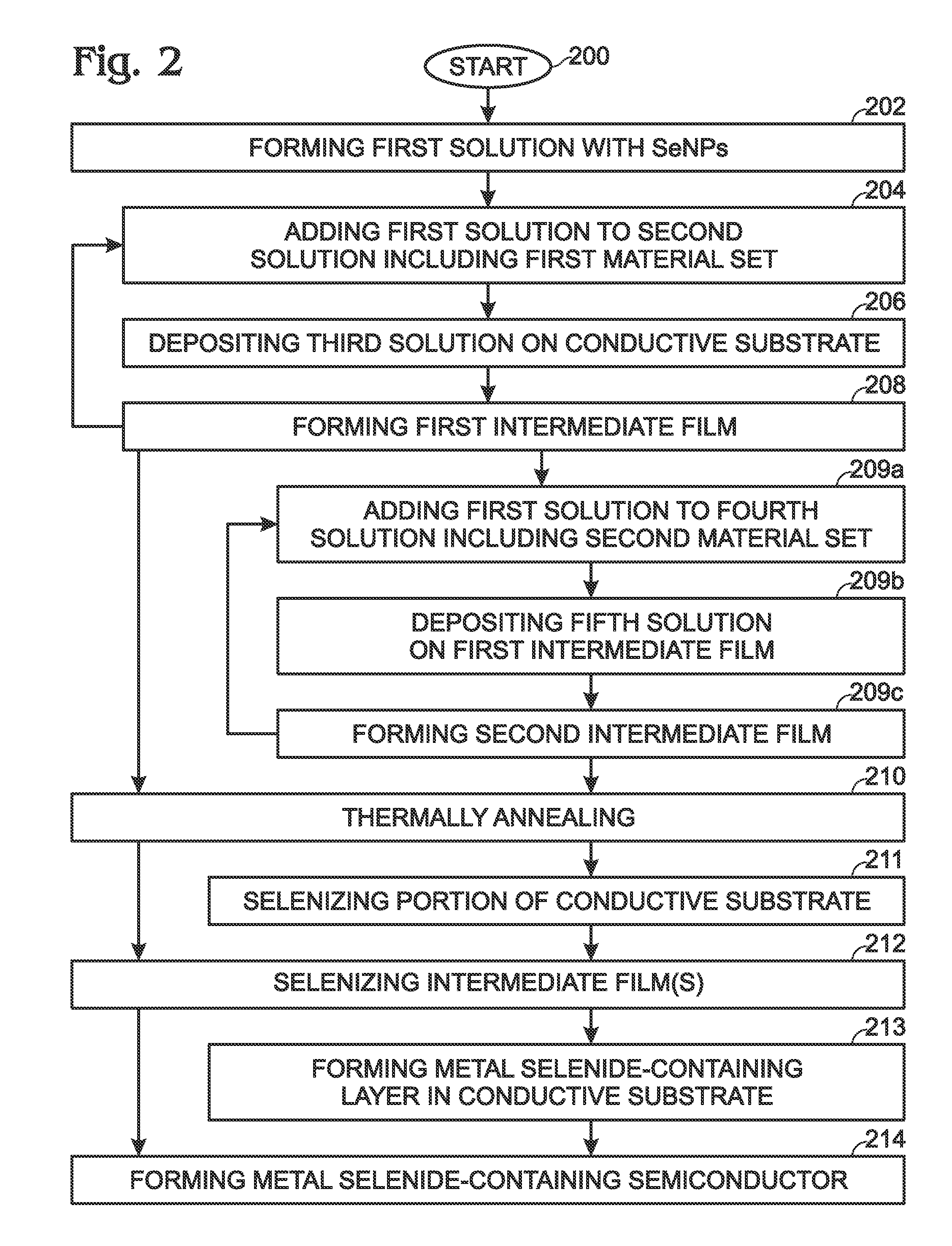
A method is provided for forming a solution-processed metal and mixed-metal selenide semiconductor using selenium (Se) nanoparticles (NPs). The method forms a first solution including SeNPs dispersed in a solvent. Added to the first solution is a second solution including a first material set of metal salts, metal complexes, or combinations thereof, which are dissolved in a solvent, forming a third solution. The third solution is deposited on a conductive substrate, forming a first intermediate film comprising metal precursors, from corresponding members of the first material set, and embedded SeNPs. As a result of thermally annealing, the metal precursors are transformed and the first intermediate film is selenized, forming a first metal selenide-containing semiconductor. In one aspect, the first solution further comprises ligands for the stabilization of SeNPs, which are liberated during thermal annealing. In another aspect, the metal selenide-containing semiconductor comprises copper, indium, gallium diselenide (CIGS).

Description

BACKGROUND OF THE INVENTION[0001]1. Field of the Invention[0002]This invention generally relates to solution based deposition processes and, more particularly, to the formation of metal selenide semiconductor films using selenium nanoparticle solutions.[0003]2. Description of the Related Art[0004]In general, metal and mixed-metal selenides represent impotent classes of semiconductor materials for electronic and photovoltaic (PV) applications. In particular, copper indium gallium diselenide (CuIn1-xGaxSe2 or CIGS) has emerged as a promising alternative to existing thin-film technologies. Overall, CIGS thin films possess a direct and tunable energy band gap, high optical absorption coefficients in the visible to near-infrared (IR) spectrum and have demonstrated power conversion efficiencies (PCEs) approaching 20%. Conventional CIGS fabrication (vacuum) processes typically involve either sequential or co-evaporation (or sputtering) of copper (Cu), indium (In), and gallium (Ga) metal on...

Claims


Application Information

Patent Timeline
IPC IPC(8): H01L21/02
CPCB82Y40/00H01L21/02568H01L21/02425H01L21/02601H01L21/02614H01L21/02628H01L31/0322Y02E10/541B82Y30/00C09D11/00C09D11/54H01L31/0326
Inventor VAIL, SEAN ANDREWKOPOSOV, ALEXEYLEE, JONG-JAN
Owner SHARP KK
Learn More