X-ray Imaging Detector, Method for Manufacturing a Photosensitive Element and an X-ray Imaging Detector
- Summary
- Abstract
- Description
- Claims
- Application Information
AI Technical Summary
Benefits of technology
Problems solved by technology
Method used
Image
Examples
Embodiment Construction
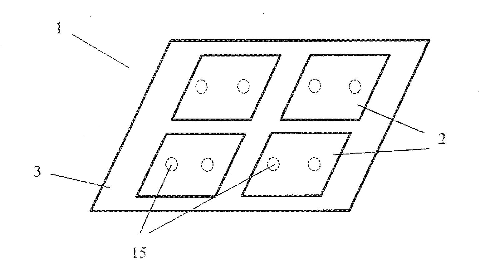
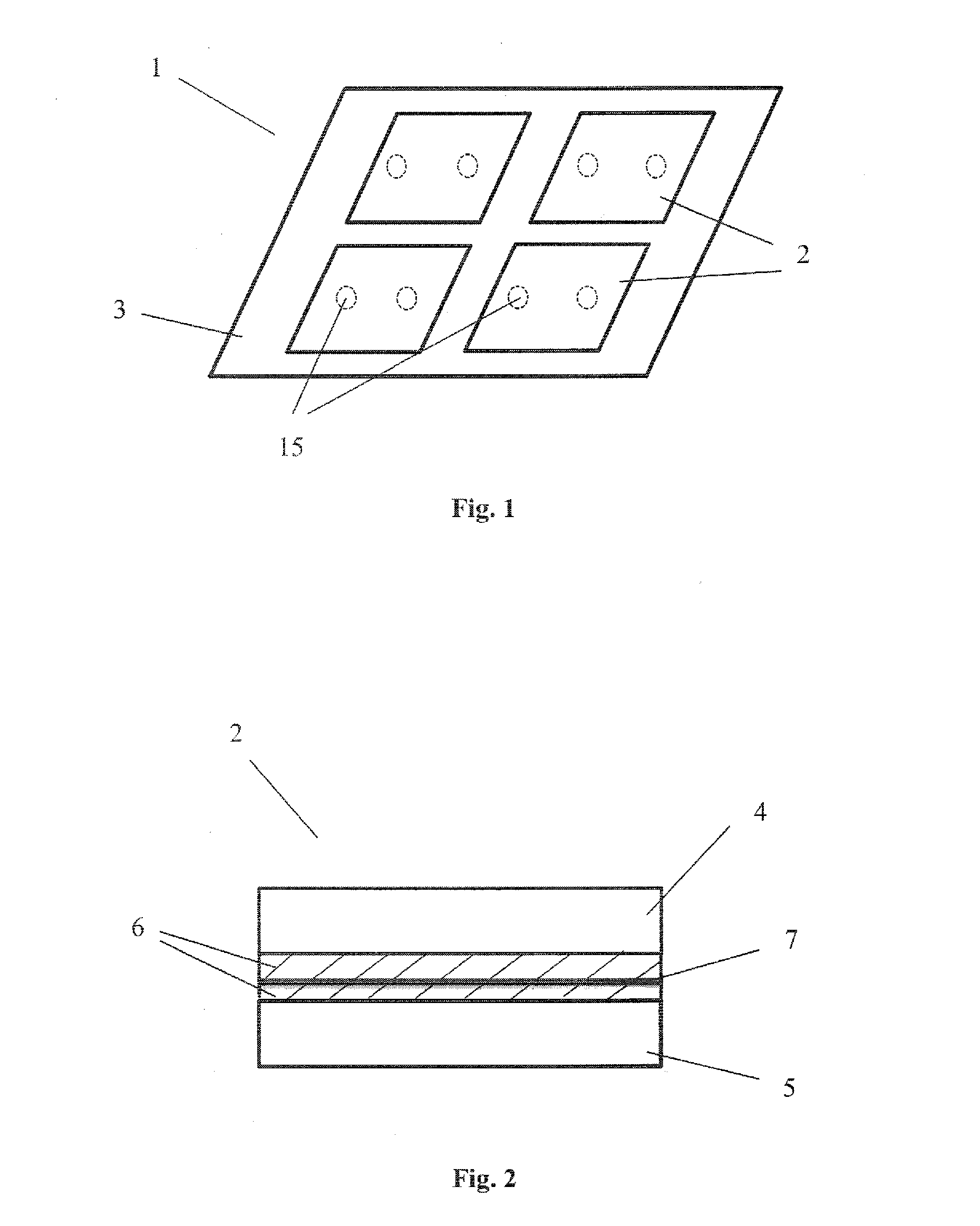
[0057]The x-ray imaging detector 1 (FIG. 1) is a multilayer structure involving a sensor array consisting of photosensitive elements 2 arranged on the common substrate 3 which can be performed out of silumin (CE7). Elements 2 are aligned in one surface in the immediate vicinity of each other forming a photosensitive surface. FIG. 1 shows one of the possible schemes to a form a sensor array with 2×2 photosensitive elements arrangement. There can be formed M×N sensor arrays where M, N≧1.
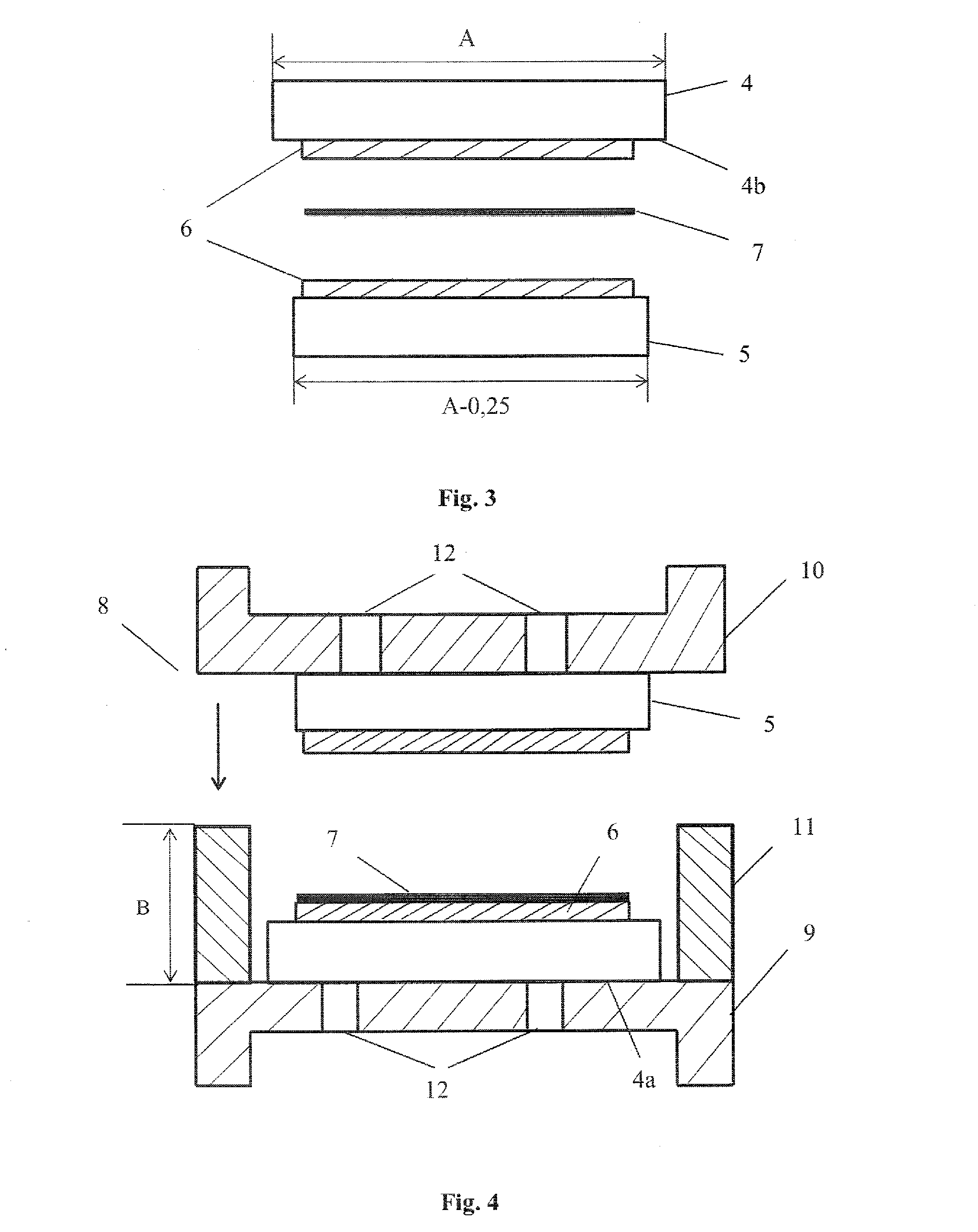
[0058]According to the claimed invention FIG. 2 schematically shows a photosensitive element 2, that similar to the detector has a multilayer structure being in reality an assemblage comprising substrate 5, performed for example out of silumin (CE7), and photosensitive plate 4 made out of silicon (Si). Between the photosensitive plate 4 and appropriate substrate 5 there is and fixed with adhesive 6 an elastically deformed interlayer 7 that can be performed as micron-scale wire mesh (stainless steel), w...
PUM
| Property | Measurement | Unit |
|---|---|---|
| Thickness | aaaaa | aaaaa |
Abstract
Description
Claims
Application Information


