Conductive films having low-visibility patterns and methods of producing the same

a technology of low-visibility patterns and conductive films, applied in the direction of superimposed coating process, resistive material coating, liquid/solution decomposition chemical coating, etc., can solve the problems of inconvenient vacuum deposition, fragile metal oxide film, prone to damage,

Active Publication Date: 2014-06-12
CHAMP GREAT INTL
View PDF0 Cites 9 Cited by
  • Summary
  • Abstract
  • Description
  • Claims
  • Application Information

AI Technical Summary

Problems solved by technology

However, metal oxide films are fragile and prone to damage when bent or otherwise subjected to physical stresses.
They also require costly processes and specialized equipment to fabricate.
Moreover, vacuum deposition is not conducive to directly forming patterns and circuits, which necessitates specialized patterning processes such as photolithography.
The specialized processes for fabricating metal oxide films put severe limitations on the substrates.
Flexible substrates (e.g., plastic), on the other hand, often fail to adhere to metal oxide as a result of moisture absorption by the substrate.
However, they generally have lower conductivity values and higher optical absorption (particularly at visible wavelengths) compared to the metal oxide films, and suffer from lack of chemical and long-term stability.

Method used


Image

  • Conductive films having low-visibility patterns and methods of producing the same
  • Conductive films having low-visibility patterns and methods of producing the same
  • Conductive films having low-visibility patterns and methods of producing the same

Examples


example 1

Synthesis of Silver Nanowires

[0071]Silver nanowires were synthesized by the reduction of silver nitrate dissolved in ethylene glycol in the presence of poly(vinyl pyrrolidone) (PVP) following the “polyol” method described in, e.g., Y. Sun, B. Gates, B. Mayers, & Y. Xia, “Crystalline silver nanowires by soft solution processing”, Nanoletters, (2002), 2(2) 165-168. A modified polyol method, described in U.S. application Ser. No. 11 / 766,552, in the name of Cambrios Technologies Corporation, produces more uniform silver nanowires at higher yields than does the conventional “polyol” method. This application is incorporated by reference herein in its entirety.

example 2

Low-Visibility Patterning

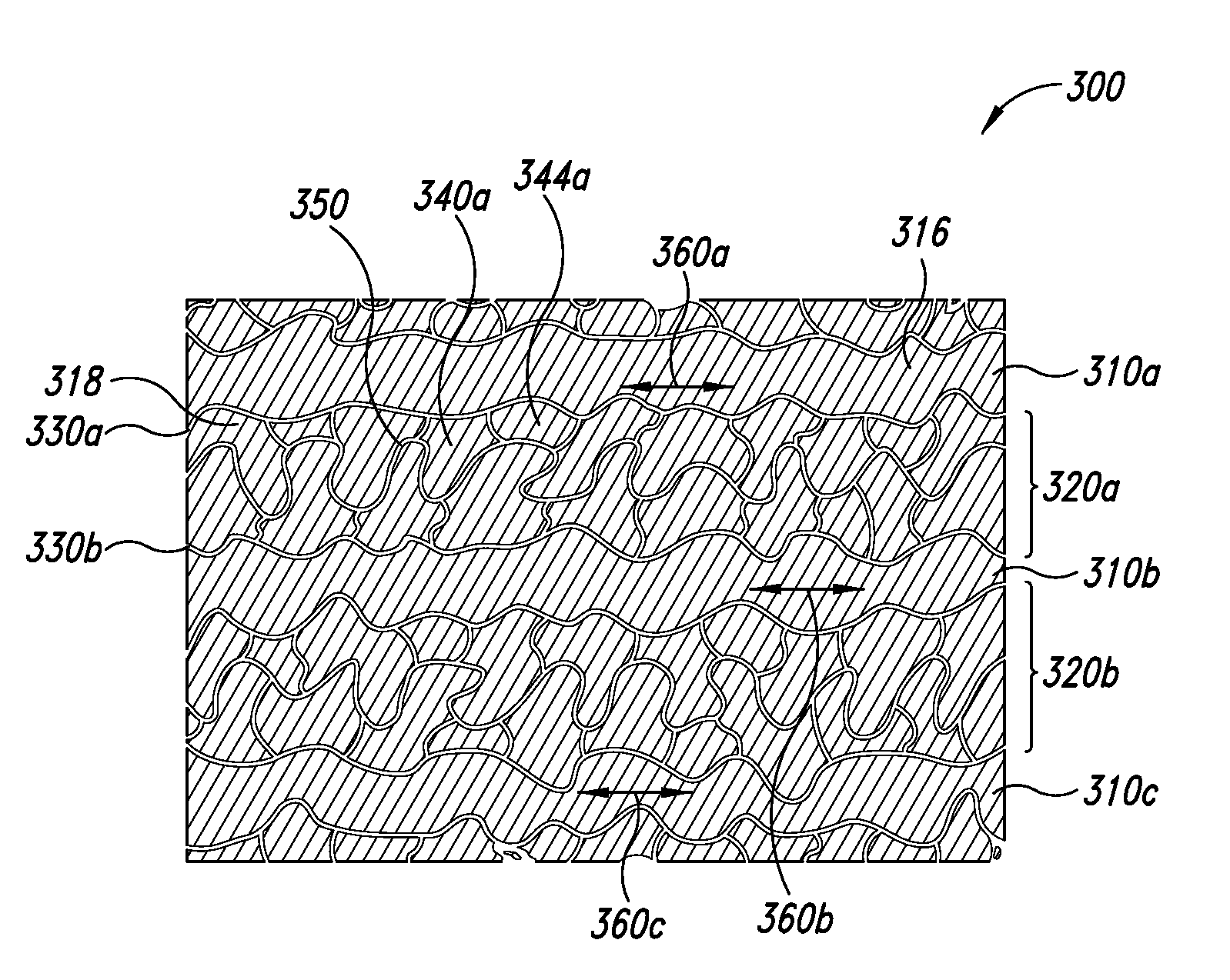
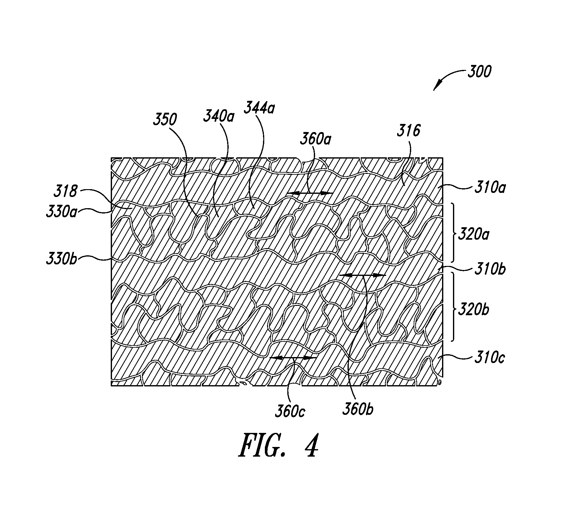
[0072]A suspension of HPMC, silver nanowires and water was prepared. The suspension was spin-coated on a glass substrate to form a thin conductive film of silver nanowires in a HPMC matrix. The conductive layer was optically clear, with an optical transmission (% T) of about 88.1% and haze (% H) of about 2.85%. The conductive layer is also highly surface-conductive with a surface resistivity of about 25Ω / □.

[0073]Thereafter, a region of the conductive film was treated with an oxidizing agent, e.g., a bleach solution having 0.5% hypochlorite, for 2 minutes. The treated film was then rinsed with water and dried in a nitrogen atmosphere. The treated region of the film showed substantially the same transmission (89.1% T) and haze (5.85% H) as compared to the optical properties of the untreated region. The treated region and the untreated region were visually uniform.

[0074]The surface resistivity of the treated region, however, has increased by several orders of m...

example 3

Photoresist Patterning Method

[0076]A silver nanowire dispersion was prepared consisting of 0.2% HPMC, 250 ppm TritonX100 and silver nanowires. The dispersion was spin-coated onto a substrate and baked for 90 seconds at 180° C. This nanowire film was then spin-coated with AZ-3330F photoresist to make a 2.5 μm transparent conducting film. The transparent conductor was then baked at 110° C. for 60 seconds. A photomask was placed in contact with a portion of the photoresist layer and the transparent conductor was exposed to light for 20 seconds at 12 mW / cm2. The conductor was then baked for 60 seconds at 110° C.

[0077]The photoresist was then developed with AZ300MIF developer, rinsed and spun dry. The conductor was then exposed to Transene silver etchant for 10 seconds, rinsed and spun dry. The photoresist was then stripped using Acetone. The transparent conductor was overcoated with Polyset PCX35-39B at 2.5% dilution in PGME and then cured for 45 min. at 180° C. The resulting patterned ...


PUM

PropertyMeasurementUnit
surface areasaaaaaaaaaa
widthaaaaaaaaaa
widthaaaaaaaaaa

Abstract

A patterned transparent conductor including a conductive layer coated on a substrate is described. More specifically, the transparent conductor has low-visibility patterns.

Description

BACKGROUNDDescription of the Related Art[0001]Transparent conductors refer to thin conductive films coated on high-transmittance surfaces or substrates. Transparent conductors may be manufactured to have surface conductivity while maintaining reasonable optical transparency. Such surface conducting transparent conductors are widely used as transparent electrodes in flat liquid crystal displays, touch panels, electroluminescent devices, and thin film photovoltaic cells; as anti-static layers; and as electromagnetic wave shielding layers.[0002]Currently, vacuum deposited metal oxides, such as indium tin oxide (ITO), are the industry standard materials to provide optical transparency and electrical conductivity to dielectric surfaces such as glass and polymeric films. However, metal oxide films are fragile and prone to damage when bent or otherwise subjected to physical stresses. They also require costly processes and specialized equipment to fabricate. Metal oxide films are typically ...

Claims


Application Information

Patent Timeline
Patent Type & Authority Applications(United States)
IPC IPC(8): H05K1/02H05K3/06
CPCH01B1/22Y10T29/49155H05K1/0296H05K3/0085H05K3/06
Inventor WOLK, JEFFREYKNAPP, MICHAEL R.
Owner CHAMP GREAT INTL
Why Eureka
Try Eureka