Method and apparatus for analyzing and for removing a defect of an EUV photomask

Active Publication Date: 2014-06-12
CARL ZEISS SMT GMBH
View PDF12 Cites 39 Cited by
  • Summary
  • Abstract
  • Description
  • Claims
  • Application Information

AI Technical Summary

Benefits of technology

[0071]If the method for the defect removal has to be used for a second time, the parameters of the repairing form are adjusted to the new situation. It may occur in this process that absorber material has to be removed or to be added only at one absorber element. The repairing form can have the parameters leading to a non-circular repairing form in order to perform s

Problems solved by technology

The EUV wavelength range presents enormous challenges to the precision of optical elements in the optical path of future lithography systems.
As a consequence of the extremely small wavelength already smallest unevenness of the multi-layer structure and minimal deviations of the absorber structure from the predetermined placement and/or of the predetermined target size of the structure elements of the absorber layer result in imaging errors of the wafers illuminated with the EUV mask.
Moreover, defects in or on the

Method used


Image

  • Method and apparatus for analyzing and for removing a defect of an EUV photomask
  • Method and apparatus for analyzing and for removing a defect of an EUV photomask
  • Method and apparatus for analyzing and for removing a defect of an EUV photomask

Examples


Example

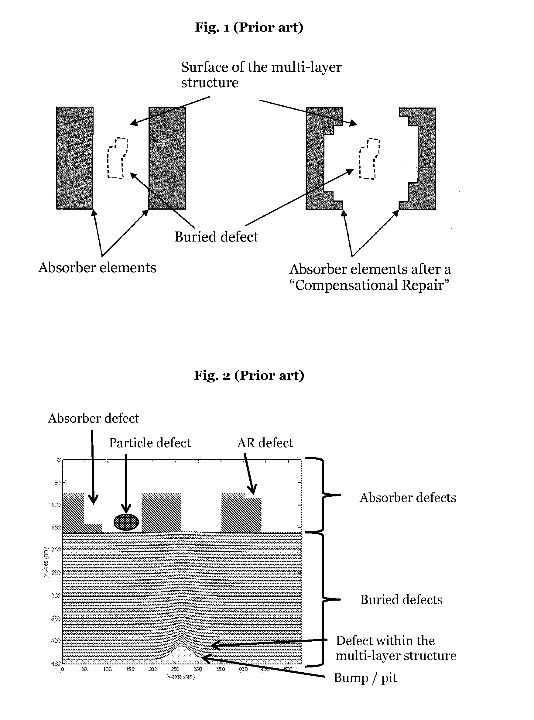
[0093]FIG. 2 gives an overview of the essential defect types of EUV masks. Absorber defects occur if absorber material is available at positions which have to be free from elements of the absorber structure. The inverse situation can also occur, i.e. the absorber material is completely or partially missing at positions which have to be covered with absorber elements. Moreover defects of the anti-reflection (AR) layer which is deposited on the absorber structure and / or dust or dirt particles on the surface of the multi-layer structure can also lead to absorber defects.

[0094]An absorber defect essentially causes an amplitude error in the reflected radiation. Typically, it can be visualized by scanning the EUV mask with a scanning electron microscope (SEM) and can be repaired with a mask repairing system, as for example a MeRiT™ system of the company Carl Zeiss. In this process missing absorber material is deposited by a local deposition process and excessive absorber material is remov...


PUM


Abstract

The invention refers to a method for analyzing a defect of an optical element for the extreme ultra-violet wavelength range comprising at least one substrate and at least one multi-layer structure, the method comprising the steps: (a) determining first data by exposing the defect to ultra-violet radiation, (b) determining second data by scanning the defect with a scanning probe microscope, (c) determining third data by scanning the defect with a scanning particle microscope, and (d) com-bining the first, the second and the third data.

Description

1. TECHNICAL FIELD[0001]The present invention relates to the field of analyzing and removing a defect of an EUV photomask.2. BACKGROUND OF THE INVENTION[0002]As a result of the constantly increasing integration density in the semiconductor industry, photolithographic masks have to project smaller and smaller structures on wafers. In order to fulfill this demand, the exposure wavelength of lithography systems has been shifted to smaller and smaller wavelengths. In the future, lithography systems will use significantly smaller wavelengths in the extreme ultra-violet (EUV) wavelength range (preferably but not exclusively in the range of 10 nm to 15 nm). The EUV wavelength range presents enormous challenges to the precision of optical elements in the optical path of future lithography systems. These optical elements are probably reflective optical elements, since the refractive indexes of presently known materials are essentially one in the EUV range.[0003]EUV mirrors comprise a substra...

Claims


Application Information

Patent Timeline
IPC IPC(8): G01Q30/02
CPCG01Q30/02G03F1/22G03F1/84G03F1/86G03F1/24B82Y10/00B82Y40/00
Inventor BUDACH, MICHAELBRET, TRISTANEDINGER, KLAUSHOFMANN, THORSTEN
Owner CARL ZEISS SMT GMBH
Why Eureka
Try Eureka