Dual-loop control for laser annealing of semiconductor wafers

a laser annealing and dual-loop technology, applied in the direction of transportation and packaging, manufacturing tools, packaging goods types, etc., can solve the problems of limiting the temperature uniformity performance of laser annealing, temperature measurement error, and unstable temperature control system, so as to reduce the noise of 1/f and reduce the variation of annealing temperature

Inactive Publication Date: 2014-06-19
VEECO INSTR
View PDF8 Cites 10 Cited by
  • Summary
  • Abstract
  • Description
  • Claims
  • Application Information

AI Technical Summary

Benefits of technology

[0011]Another aspect of the disclosure is a laser annealing system for annealing dies supported by a wafer having a surface that supports dies each having a variation in emissivity. The system includes a chuck that supports the wafer, and a movable stage that supports the chuck and that is adapted to move the chuck and wafer. The system also has a laser that generates an initial laser beam and that has an adjustable output power and 1 / f noise. The system further includes an optical system configured to receive the initial laser beam and form therefrom an annealing laser beam and to direct a portion of the annealing laser beam to a photodetector system that in response generates a detector signal. The optical system is arranged so that the annealing laser beam is made incident upon and scans over the wafer surface due to the movement of the wafer, and heats the wafer to an annealing temperature. The system also includes a thermal emission detector system arranged relative to the wafer surface and configured to receive thermal emission radiation therefrom that is generated by the annealing laser beam and average the received thermal emission radiation over an area of one or more of the dies, and in response generates a thermal emission signal. The system also has a first control loop configured to receive the detector signal and control the laser to adjust the output power at a first frequency f1 in the range from 1 kHz to 100 kHz to reduce the 1 / f noise. The system further has a second control loop configured to receive the thermal emission signal and control the laser to adjust the output power at a second frequency f2 in the range from 1 Hz to 100 Hz to reduce variations in the annealing temperature.

Problems solved by technology

Local emissivity variations on patterned wafers can cause a temperature measurement error when the system cannot distinguish between a change in emission due to true temperature change and a local change in emissivity.
Consequently, as the laser annealing beam scans such wafers, the amplitude and time-frequency of the pattern-induced emission variation is such that the temperature control system can become unstable.
As a result, the laser annealing system must process silicide and memory wafers in open loop (constant laser power) condition, which limits the temperature uniformity performance of the laser anneal due to the uncompensated effects such as laser power density fluctuation and / or variation in the local substrate temperature.
This in turn limits the maximum safe annealing temperature.
This presents a process compromise when (as is the case in most spike anneal process applications) a higher anneal temperature (below damage threshold) produces a superior process result

Method used


Image

  • Dual-loop control for laser annealing of semiconductor wafers
  • Dual-loop control for laser annealing of semiconductor wafers
  • Dual-loop control for laser annealing of semiconductor wafers

Examples


Embodiment Construction

[0019]Reference is now made in detail to embodiments of the disclosure, examples of which are illustrated in the accompanying drawings. Whenever possible, the same or like reference numbers and symbols are used throughout the drawings to refer to the same or like parts.

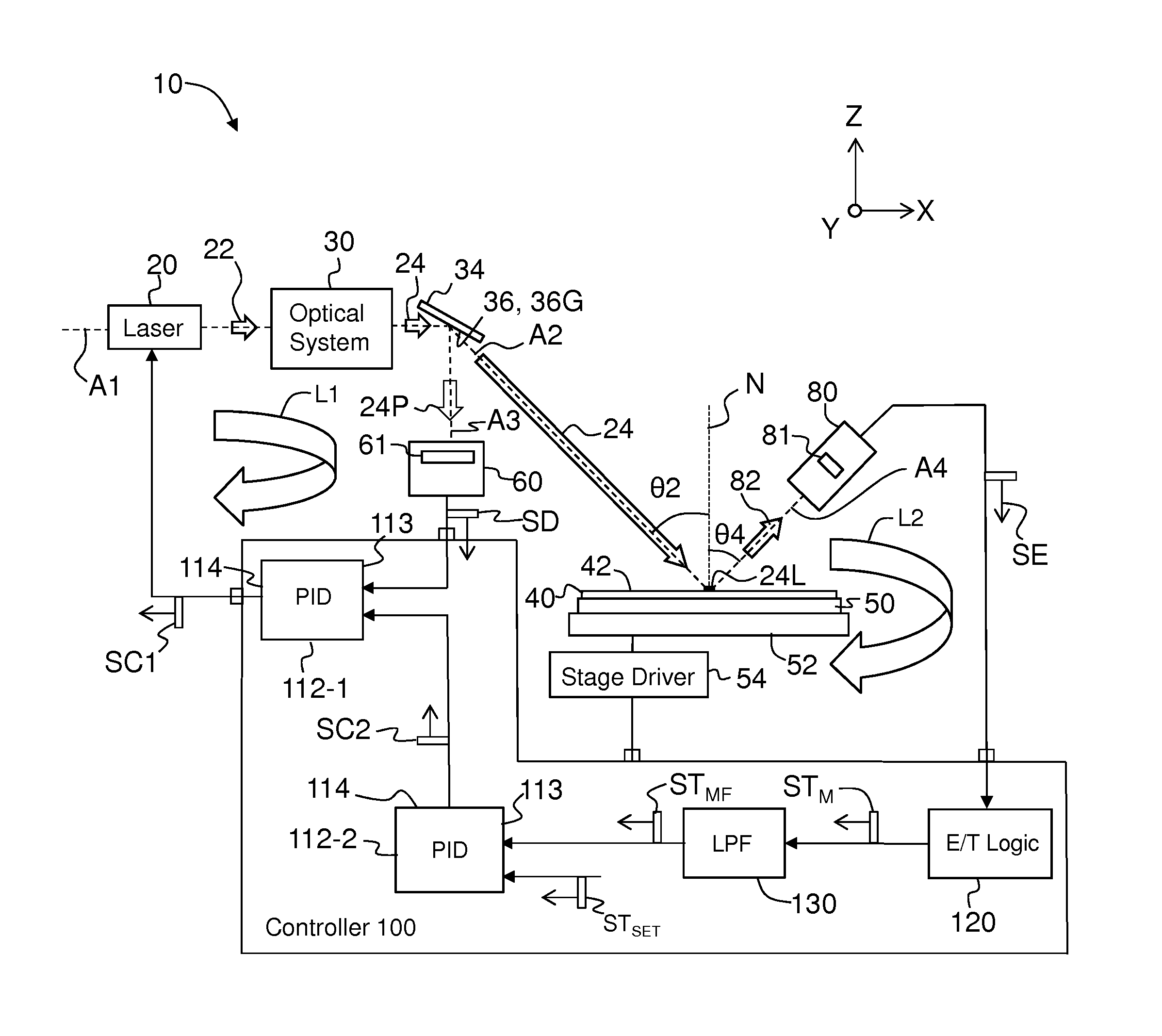
[0020]FIG. 1 is a schematic diagram of an example laser annealing system 10 that illustrates an embodiment of the dual-loop control configuration for the system. A Cartesian coordinate system is shown for the sake of reference. Example laser annealing systems 10 are described, for example, U.S. Pat. Nos. 7,612,372, 7,154,066 and 6,747,245, and U.S. Patent Application Publications No. 2010 / 0084744 and 2012 / 0100640, all of which are incorporated by reference herein.

[0021]System 10 includes laser 20 that emits an initial laser beam 22 along an optical axis A1 that runs in the X-direction. An example laser 20 is a CO2 laser that emits light at a nominal annealing wavelength λA of 10.6 μm. Laser 20 may also consist of or i...


PUM

PropertyMeasurementUnit
frequency f1aaaaaaaaaa
frequency f2aaaaaaaaaa
temperatureaaaaaaaaaa

Abstract

Systems and methods for performing semiconductor laser annealing using dual loop control are disclosed. The first control loop operates at a first frequency and controls the output of the laser and controls the 1 / f laser noise. The second control loop also controls the amount of output power in the laser and operates at second frequency lower than the first frequency. The second control loop measures the thermal emission of the wafer over an area the size of one or more die so that within-die emissivity variations are average out when determining the measured annealing temperature. The measured annealing temperature and an annealing temperature set point are used to generate the control signal for the second control loop.

Description

CROSS-REFERENCE TO RELATED APPLICATIONS[0001]This application is a divisional application of co-pending U.S. patent application Ser. No. 13 / 706,397, filed on Dec. 6, 2012, from which priority is claimed and which is incorporated by reference herein.FIELD[0002]The present disclosure relates generally to laser annealing of semiconductors, and in particular relates to dual-loop control for semiconductor laser annealing.BACKGROUND ART[0003]Laser annealing (also called laser spike annealing or laser thermal processing) is used in semiconductor manufacturing for a variety of applications, including for activating dopants in select regions of devices (structures) formed in a semiconductor wafer when forming active microcircuits such as transistors.[0004]One form of laser annealing uses a scanned laser beam (“laser annealing beam”) to heat the surface of the wafer to a temperature (the “annealing temperature”) for a time long enough to activate the dopants in the semiconductor structures (e...

Claims


Application Information

Patent Timeline
Patent Type & Authority Applications(United States)
IPC IPC(8): B23K26/00
CPCB65D5/02B65D5/0281B65D5/029B65B21/24B65D81/03B23K26/352
Inventor MCWHIRTER, JAMES T.GAINES, DAVIDLEE, JOSEPHZAMBON, PAULO
Owner VEECO INSTR
Why Eureka
Try Eureka