Silicon-on-insulator radio frequency device and silicon-on-insulator substrate

a radio frequency device and silicon-on-insulator technology, applied in the field of silicon-on-insulator radio frequency devices and silicon-on-insulator substrates, can solve the problems that the loss and linearity of signals in conventional soi rf devices cannot meet the application requirements, the loss of rf signals may be great, and the loss of rf signals may be poor. achieve high resistivity, increase an equivalent surface resistance, and high resistivity

Active Publication Date: 2014-06-26
SHANGHAI HUAHONG GRACE SEMICON MFG CORP
View PDF8 Cites 15 Cited by
  • Summary
  • Abstract
  • Description
  • Claims
  • Application Information

AI Technical Summary

Benefits of technology

[0043]Compared with the conventional solutions, the present disclosure may have following advantages.
[0044]In the SOI RF device provided in the present disclosure, a pit is formed on a surface of a high resistivity silicon plate which is close to a buried oxide layer. The pit may be filled with an insulating material, thereby increasing an equivalent surface resistance of the high resistivity silicon plate; or no insulating material is filled into the pit, that is, the pit remains a vacuum state or is only filled with air, which can increase the equivalent surface resistance of the high resistivity silicon plate as well. In such, an eddy current generated on a surface of the high resistivity silicon plate under the action of a RF signal may be reduced. As a result, loss of the RF signal may be reduced and the linearity of the RF signal may be improved.

Problems solved by technology

However, in practice, especially in RF applications which require high linearity and low insertion loss, if the above SOI RF device is employed, loss of RF signals may be great and linearity of the RF signals may be poor.
In some RF applications which require high linearity and low insertion loss, loss and linearity of signals in conventional SOI RF devices cannot reach application requirements.

Method used


Image

  • Silicon-on-insulator radio frequency device and silicon-on-insulator substrate
  • Silicon-on-insulator radio frequency device and silicon-on-insulator substrate
  • Silicon-on-insulator radio frequency device and silicon-on-insulator substrate

Examples


Embodiment Construction

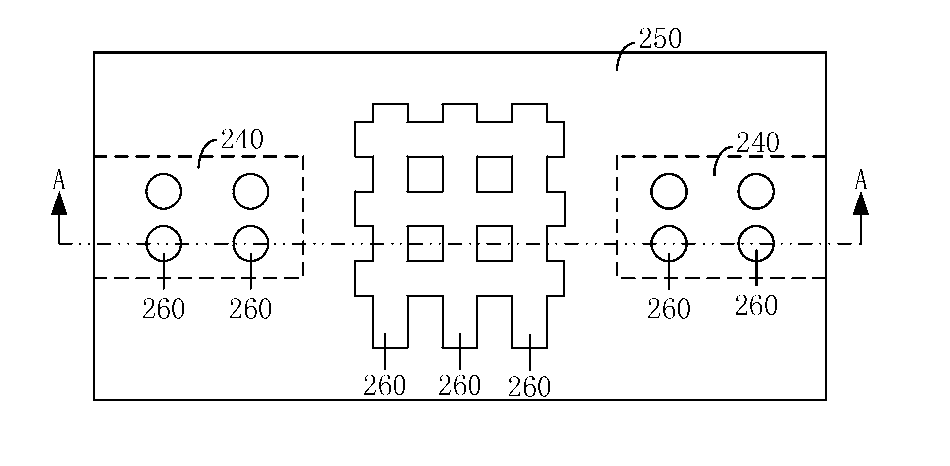
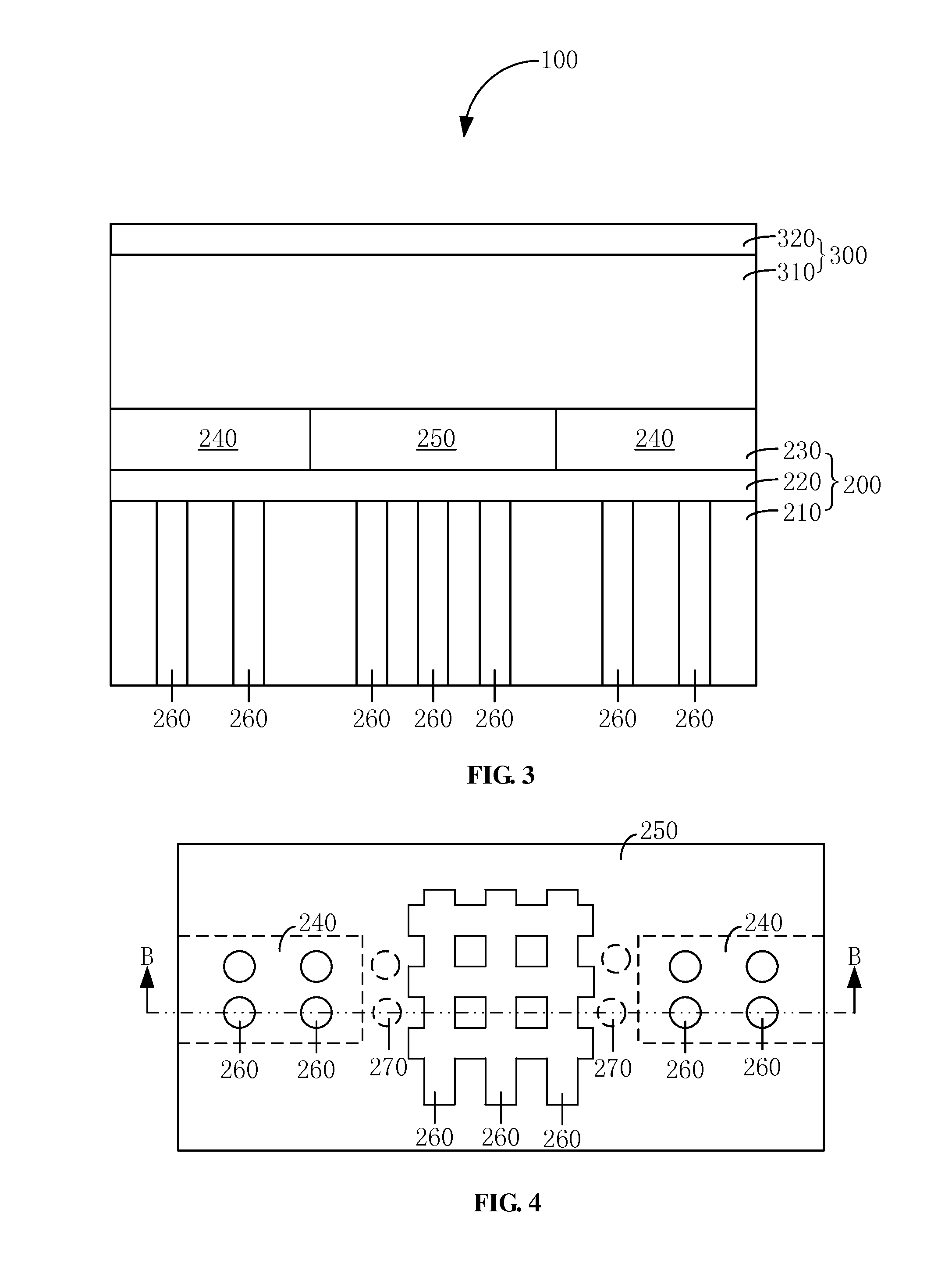
[0055]In some RF applications which require high linearity and low insertion loss, loss and linearity of RF signals in conventional SOI RF devices cannot meet the application requirements. In embodiments of the present disclosure, in a SOI substrate which is used to form a RF device, at least one pit is formed on a surface of a high resistivity silicon plate which is close to a buried oxide layer to increase an equivalent surface resistance of the high resistivity silicon plate. Therefore, an eddy current generated on a surface of the high resistivity silicon plate under the action of a RF signal may be reduced. As a result, loss of the RF signals may be reduced and the linearity of the RF signals may be improved.

[0056]In order to clarify the objects, characteristics and advantages of the disclosure, embodiments of present disclosure will be described in detail in conjunction with accompanying drawings. The following embodiments are only illustrative. Those skilled in the art can mo...


PUM


Abstract

A silicon-on-insulator radio frequency device and a silicon-on-insulator substrate are provided. In the silicon-on-insulator radio frequency device, a pit is formed on a surface of a high resistivity silicon plate which is close to a buried oxide layer. The pit may be filled with an insulating material, thereby increasing an equivalent surface resistance of the high resistivity silicon plate; or no insulating material is filled into the pit, that is, the pit remains a vacuum state or is only filled with air, which can increase the equivalent surface resistance of the high resistivity silicon plate as well. In such, an eddy current generated on a surface of the high resistivity silicon plate under the action of a radio frequency signal may be reduced. As a result, loss of the radio frequency signal is reduced and the linearity of the radio frequency signal is improved.

Description

CROSS-REFERENCE TO RELATED APPLICATIONS[0001]The present application claims priority to Chinese patent application No. 201210564175.6, filed on Dec. 21, 2012, and entitled “SILICON-ON-INSULATOR RADIO FREQUENCY DEVICE AND SILICON-ON-INSULATOR SUBSTRATE”, and the entire disclosure of which is incorporated herein by reference.FIELD OF THE DISCLOSURE[0002]The present disclosure generally relates to semiconductor manufacturing, and more particularly, to a silicon-on-insulator radio frequency device and a silicon-on-insulator substrate.BACKGROUND OF THE DISCLOSURE[0003]Semiconductor devices are developed to have higher integration, higher speed and lower power consumption, which limit the application of bulk silicon substrates more and more. On the contrary, Silicon-On-Insulator (SOI) substrates can realize dielectric isolation of components in an integrated circuit, avoid a latch-up effect in a bulk silicon Complementary Metal Oxide Semiconductor (CMOS) circuit, have the advantages of sm...

Claims


Application Information

Patent Timeline
Patent Type & Authority Applications(United States)
IPC IPC(8): H01L29/06
CPCH01L29/0649H01L21/76283H01L21/84H01L27/1203
Inventor LI, ERNESTXU, DANIEL
Owner SHANGHAI HUAHONG GRACE SEMICON MFG CORP
Why Eureka
Try Eureka