Transparent polymeric electrodes for electro-optical structures, processes for producing the same, and dispersions used in such processes

a technology of transparent polymeric electrodes and electrooptical structures, which is applied in the direction of sustainable manufacturing/processing, non-metal conductors, final product manufacturing, etc., can solve the problems of not being able to use very thin lighting elements, and not being able to achieve the same

Active Publication Date: 2011-05-10
HERAEUS PRECIOUS METALS GMBH & CO KG
View PDF17 Cites 15 Cited by
  • Summary
  • Abstract
  • Description
  • Claims
  • Application Information

AI Technical Summary

Benefits of technology

[0114]a) In OLEDs and OSCs, for example, there is no need for TCO layers, such as ITO for example, or thin metal layers.
[0115]b) In the case of flexible substrates, bending the substrate does not lead to cracks in the brittle TCO layers and a failure of the electro-optical structure, since these polymeric layers are very ductile and flexible.
[0116]c) Organic layers are simpler to structure than inorganic layers, such as ITO for example. Organic layers can be removed again with solvents, by optical irradiation (UV) or by thermal irradiation (laser ablation).
[0117]The double-layer electrode according to the invention comprising a first and second layer also shows clear advantages over known polymer electrodes. In particular, thanks to the fine particle structure and low surface roughness, the short-circuit probability for OLEDs and OSCs is reduced considerably with the electrodes according to the invention. The significantly increased conductivity of the first electrode layer is also surprising, since it is known from the literature that reducing the particle size increases the surface resistance of resulting layers (A. Elschner et al., Asia Display IDW 2001, OEL 3-3, p. 1429). Even adding conductivity-increasing additives should not be expected to compensate for this negative influence of particle refinement on conductivity, let alone further increase the conductivity. The electroluminescence efficiency in OLEDs can be increased significantly through the use of the electrodes according to the invention. In particular, using the electrodes according to the invention in accordance with the particularly preferred embodiments, wherein both the first and the second electrode layer contains PEDT:PSA, an increase in electroluminescence efficiency of 1 to 3 orders of magnitude can be achieved as compared with single-layer electrodes with the same device current.
[0118]The effect obtained is unexpected, since in both layers the only electrically active component is the electrically conductive polythiophene, whereas the polymeric anions are electrically inert and primarily serve to keep the electrically conductive polymer or polythiophene in solution during polymerisation and the conductivity-increasing additives substantially volatise at drying temperatures of over 120° C.
[0119]To keep the voltage drop between the anode contact point and the OLED anode especially low, highly conductive leads made from metals, for example, and known as busbars can be used.
[0120]In the case of passive matrix OLED displays, ITO address lines can be dispensed with on account of the invention. In their place, metal leads (busbars) in combination with the electrode according to the invention carry out anode-side addressing (see FIG. 1). Electrical leads 2a and pixel frames 2b with high conductivity are applied to a transparent support 1, e.g. a glass plate. They could be applied for example by vapour deposition of metals or inexpensively by printing with metal pastes. The polymeric electrode layer 3 is then deposited into the frames. An adhesion promoter is optionally applied first, then the first electrode layer and finally the second electrode layer. These layers are preferably applied by spin coating, printing and inkjet printing. The remaining structure corresponds to that of a standard passive matrix OLED and is known to the person skilled in the art.
[0121]In the case of homogeneously illuminating OLEDs (OLED lamps), ITO electrodes can be dispensed with on account of the invention. In their place, metal leads (busbars) in combination with the electrode according to the invention assume the function of the full-surface anode (see FIG. 2). Electrical leads 2 with high conductivity are applied to a transparent support 1, e.g. a glass plate, in the manner described in the previous paragraph, for example. The polymeric electrode layer 3 is then deposited on top in the sequence described in the previous paragraph. The remaining structure corresponds to that of a standard OLED lamp.
[0122]The dispersions which are particularly suitable for producing the first electrode layer are likewise not known from the literature and are thus provided by the present invention.

Problems solved by technology

Due to their extremely flat design, they can be used to build very thin lighting elements, which hitherto was not possible.
Neither OLED displays nor OLED lighting elements are limited to a flat, rigid design.
The economic success of these novel electro-optical structures will depend not only on fulfilment of the technical requirements but substantially also on manufacturing costs.
The deposition of these inorganic layers takes place by sputtering, reactive surface atomisation (reactive sputtering) or thermal evaporation of the organic material in vacuo and is therefore complex and cost-intensive.
ITO layers are a substantial cost factor in the production of OLEDs or OSCs.
a) ITO can only be deposited in a complex, cost-intensive vacuum process (by reactive sputtering).
b) Temperatures of T>400° C. are necessary in the deposition process if high conductivities are to be obtained. In particular, the polymer substrates which are important for flexible displays do not withstand these temperatures.
c) ITO is brittle and forms cracks when shaped.
d) The metal indium is a raw material with only limited production, and supply shortages are predicted if consumption increases further.
e) The environmentally compatible disposal of electro-optical structures containing the heavy metal indium is a problem which has yet to be solved.
Despite these disadvantages, ITO layers are still used because of their favourable ratio of electrical conductivity to optical absorption and above all due to the lack of suitable alternatives.
Alternatives to ITO as electrode materials have been discussed in the past, but hitherto no alternatives have been found which do not exhibit the disadvantages described above and which at the same time offer comparably good properties in electro-optical structures.
However, as well as being likewise difficult to process on the substrate, these in-situ-PEDT layers have the disadvantage, particularly for applications in OLEDs, that firstly the material has a strong inherent colour and secondly that the electroluminescence efficiencies that can be achieved with it are low.
However, the conductivity of PEDT:PSA layers produced from formulations having a PEDT:PSA ratio such as 1:2.5 (percent by weight) is not particularly high, e.g. approx.
Furthermore, the fact that these formulations lead to relatively rough layer surfaces because of their coarse particle structure argues against the use of these layers as an ITO substitute in many electro-optical applications.
In particular, for applications which are sensitive to short-circuits due to surface roughness, such as OLEDs and OSCs, these layers are thus not very suitable.

Method used


Image

  • Transparent polymeric electrodes for electro-optical structures, processes for producing the same, and dispersions used in such processes
  • Transparent polymeric electrodes for electro-optical structures, processes for producing the same, and dispersions used in such processes
  • Transparent polymeric electrodes for electro-optical structures, processes for producing the same, and dispersions used in such processes

Examples


example 1

Production of a PEDT:PSA Dispersion for Producing the First Electrode Layer:

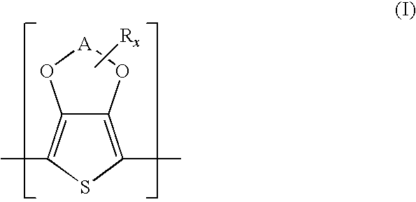
[0129]a) (According to the invention) In a commercially obtainable aqueous polyethylenedioxythiophene / polystyrene sulfonic acid dispersion (PEDT:PSA dispersion) with a polyethylenedioxythiophene / polystyrene acid weight ratio of 1:2.5, a solids content of approx. 1 wt. % and a viscosity of approx. 300 mPas at a shear rate of 100 s−1 and at 20° C. (Baytron® PHC V4 from H.C. Starck GmbH), a particle size distribution with a d50 value of 25 nm, i.e. 50 wt. % of the particles smaller than 25 nm, was established by homogenisation. The dispersion was then concentrated from approx. 1 wt. % to a solids content of 1.7 wt. %, filtered (Pall, pore size: 0.2 μm) and then mixed with 5 wt. % dimethyl sulfoxide (DMSO). The viscosity of this solution was approx. 45 mPas at a shear rate of 100 s−1 and at 20° C.

[0130]b) (Comparative example) A commercially obtainable aqueous PEDT:PSA dispersion with a polyethylenedioxythiophen...

example 2

Production and Characterisation of a First Electrode Layer:

[0132]a) (According to the invention) Glass substrates were cut to a size of 50×50 mm2, cleaned and activated for 15 minutes with UV / ozone. The dispersion from example 1a) was then distributed over the glass substrate by means of a spin coater at the specified spin speed and an acceleration of 500 rpm / sec for 30 seconds. Parallel silver contacts were vapour deposited using a shadow mask and the surface resistance was determined. The film thickness was determined with a stylus profilometer (Tencor 500), the surface roughness with a scanning force microscope (Digital Instruments).

[0133]b) (Comparative example) Glass substrates were prepared as described in 2a), coated with a dispersion from example 1b) and their standard colour value, surface resistance, film thickness and surface roughness were determined.

[0134]c) (Comparative example) Glass substrates were prepared as described in 2a), coated with a dispersion from example 1...

example 3

Production of an OLED without a Second Electrode Layer

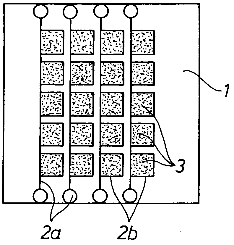
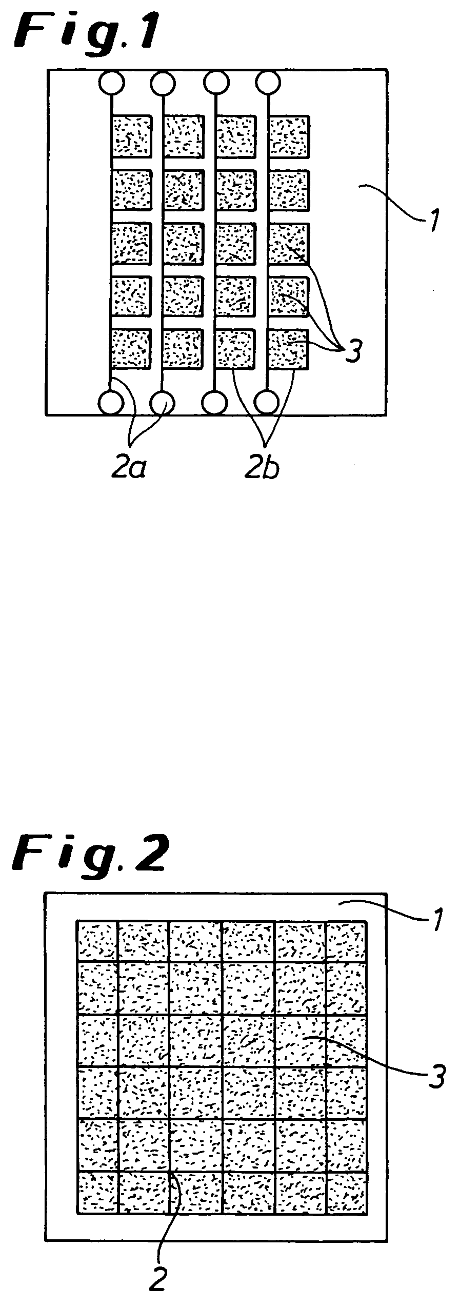
[0137]1. Substrates with Metallic Fingers:

[0138]Glass substrates were cut to a size of 50×50 mm2 and cleaned. Then metal fingers in silver were vapour deposited onto the substrate using a shadow mask. The parallel metal lines with a width of 1 mm and a distance of 5 mm apart were connected by means of a central bar running perpendicular to them and had a height of 170 nm. Immediately before coating, the substrate surfaces were cleaned and activated with UV / ozone (UVP Inc., PR-100) for 15 minutes.

[0139]2. Application of a First Electrode Layer Using a PEDT:PSA Dispersion According to the Invention:

[0140]Approx. 2 ml of the dispersion from example 1a) were poured onto the substrate and then distributed on the glass substrate with the metal fingers using a spin coater at 1000 rpm and an acceleration of 500 rpm / sec for 30 seconds. The substrate with the still wet electrode layer was then placed on a hot plate, covered with a Petri di...


PUM

PropertyMeasurementUnit
surface roughness Raaaaaaaaaaa
electrical conductivityaaaaaaaaaa
surface roughness Raaaaaaaaaaa

Abstract

The invention concerns a process for producing transparent multi-layer electrodes from conductive polymers, electrodes produced by this process and their use in electro-optical structures.

Description

BACKGROUND OF THE INVENTION[0001]Owing to their particular properties, displays based on organic light-emitting diodes (OLEDs) are an alternative to the established technology of liquid crystals (LCD). This novel technology offers advantages in particular in applications involving portable devices which are not plugged into the mains supply, such as mobile telephones, pagers and toys, for example.[0002]The advantages of OLEDs include the extremely flat design, the property of generating their own light, which means that like liquid crystal displays (LCDs) they require no additional light source, the high luminous efficiency and the unrestricted viewing angle.[0003]In addition to displays, however, OLEDs can also be used for lighting purposes, for example in large-area radiation emitters. Due to their extremely flat design, they can be used to build very thin lighting elements, which hitherto was not possible. The luminous efficiencies of OLEDs now exceed those of thermal radiation e...

Claims


Application Information

Patent Timeline
Patent Type & Authority Patents(United States)
IPC IPC(8): H01B1/12
CPCC08G61/123C08G61/126H01B1/127H01L51/0021H01L51/0037H01L51/441H01L51/5206H01L2924/0002Y02E10/549H01L2924/00Y10T428/31533Y02P70/50H10K59/179H10K71/60H10K85/1135H10K30/81H10K50/17H10K50/81H10K50/816H05B33/20H05B33/26
Inventor ELSCHNER, ANDREASLOEVENICH, PETER WILFRIEDJONAS, FRIEDRICH
Owner HERAEUS PRECIOUS METALS GMBH & CO KG
Why Eureka
Try Eureka