Dynamic voltage scaling system having time borrowing and local boosting capability

a voltage scaling and dynamic technology, applied in the field of dynamic voltage scaling system, can solve the problems of circuit operation fault, circuit cannot realize effective voltage scaling, power consumption is raised, etc., and achieve the effect of reducing power consumption, raising circuit performance, and reducing data throughput of the system

Active Publication Date: 2014-06-26
NATIONAL CHUNG CHENG UNIV
View PDF5 Cites 9 Cited by
  • Summary
  • Abstract
  • Description
  • Claims
  • Application Information

AI Technical Summary

Benefits of technology

[0012]A major objective of the present invention is to provide a dynamic voltage scaling system having time borrowing and local boosting capability. Wherein, a latch is utilized to perform time borrowing for the next stage pipeline logic circuit, meanwhile, it local boosts the working voltage of the next stage pipeline logic circuit, to solve delay fault problem of the pipeline.
[0013]Another objective of the present invention is to provide a dynamic voltage scaling system having time borrowing and local boosting capability. Wherein, the delay fault in the DVS system of the prior art is solved effectively without reducing data throughput of the system.
[0014]A further objective of the present invention is to provide a dynamic voltage scaling system having time borrowing and local boosting capability, that is capable of raising circuit performance, reducing power consumption, lowering process variations, to achieve dynamic voltage scaling effectively.
[0015]In order to achieve the above objective, the present invention provides a dynamic voltage scaling system having time borrowing and local boosting capability, including: a time borrowing circuit, and a local boost circuit. Wherein, the time borrowing circuit is connected electrically between a primary stage logic circuit and a secondary stage logic circuit. The local boost circuit is connected electrically to the time borrowing circuit and the secondary stage logic circuit. Wherein, the time borrowing circuit receives an all-domain clock signal, and generates an output data to the secondary stage logic circuit based on data input to the primary stage logic circuit. When the data input to the time borrowing circuit lags behind the positive level of the all-domain clock signal, time borrowing circuit delays data fetching of the flip flop, so that the primary stage pipeline can perform time borrowing for the secondary stage pipeline. Normally, the local boost circuit is connected electrically to a low working voltage line when the input data lags behind the positive level of the all-domain clock signal, the time borrowing circuit changes its status and produces a warning signal, so that the local boost circuit disconnects its connection to the low working voltage line based on the warning signal, and it is connected electrically to a high working voltage line, to reduce the operation time of the secondary stage pipeline.
[0016]According to an embodiment of the present invention, when the time borrowing circuit produces a warning signal, the circuit utilizes a latch to perform time borrowing through the next stage pipeline; meanwhile, it is connected to a high working voltage line through the local boost circuit, to raise its working voltage, offset its delay fault, and reduce its power consumption.
[0017]Furthermore, in order to assure that the next stage pipeline can still operate properly, when performing time borrowing, the latch itself informs a stage delay reduction circuit to reduce time delay of the next stage pipeline. By employing the stage delay reduction circuit, the time borrowed by the primary stage pipeline can be offset and its power consumption can be reduced as well. In one embodiment of the present invention, the stage delay reduction circuit can be implemented by boosting supply voltage. In another embodiment of the present invention, the stage delay reduction circuit can also be implemented by forwarding body-bias

Problems solved by technology

Along with the progress and development of its manufacturing process, the circuit density and performance of microprocessor have increased significantly, so that its power consumption is raised.
Otherwise, in case the time delay of signal CP passing through CPM 2 does exceed the clock period of the system, then the system is in an under-voltage condition, such that the circuit may operate in fault.
However, considering the process variations, CPM 2 must reflect the harmful voltage before an error does occur in the logic circuit.
In this way, the circuit can not realize effective voltage scaling, thus not being able to save power consumption efficiently.
However, it is worth to note that, regardless of Razor-I or Razor-II, when system error occurs, Data Recovery or Instruction Replay must be performed, to bring the system back to normal operation, such that this approach of solving system error requires an additional cycle period or tens of cycle periods.
When this happens to a large system work load, it could greatly reduce system data throughput, to affect seriously performance of the system.
Therefore, presently, the design and performance of the dynamic voltage scaling system is not quite satisfactory, and it has much room for improvements.

Method used


Image

  • Dynamic voltage scaling system having time borrowing and local boosting capability
  • Dynamic voltage scaling system having time borrowing and local boosting capability
  • Dynamic voltage scaling system having time borrowing and local boosting capability

Examples


Embodiment Construction

[0034]The purpose, construction, features, functions and advantages of the present invention can be appreciated and understood more thoroughly through the following detailed description with reference to the attached drawings.

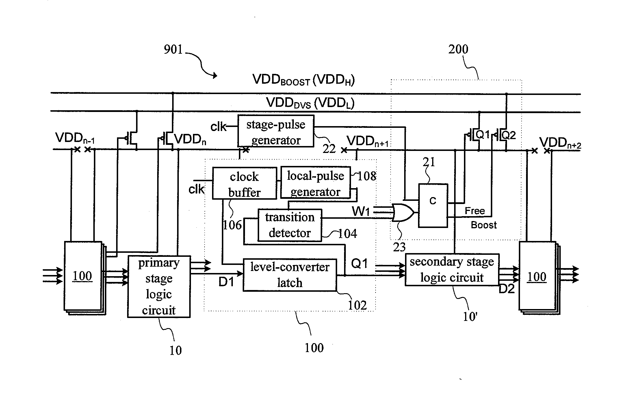
[0035]The present invention relates to a Dynamic Voltage Scaling (DVS) system having Time borrowing and Local Boosting capability, that is different from the prior art in that, in the present invention, when a delay fault occurs, the system will not stop to solve the delay fault problem. Instead, it utilizes a latch to borrow operation time from the next stage pipeline. Meanwhile, it can raise the operation voltage of the next stage pipeline to offset this delay fault, hereby raising significantly data throughput of the system.

[0036]Refer to FIG. 3 for a circuit diagram of a Dynamic Voltage Scaling (DVS) system capable of Time borrowing and Local Boosting according to the present invention. As shown in FIG. 3, the Dynamic Voltage Scaling (DVS) system 901 includ...


PUM


Abstract

A dynamic voltage scaling system having time borrowing and local boosting capability, including: a time borrowing circuit and a local boost circuit. The time borrowing circuit connected electrically between a primary stage logic circuit and a secondary stage logic circuit is activated by an all-domain clock signal, and then generates an output data to the secondary stage logic circuit based on input data to the primary stage logic circuit. The local boost circuit is connected to a low working voltage line, when input data of the time borrowing circuit lags behind a positive level of said all-domain clock signal, the time borrowing circuit delays fetching data by a flip flop and changes state to produce a warning signal, so that the local boost circuit disconnects its connection with said low working voltage line, and is connected electrically to a high working voltage line.

Description

[0001]This application claims priority for Taiwan patent application no. 101149022 filed on Dec. 21, 2012, the content of which is incorporated by reference in its entirety.BACKGROUND OF THE INVENTION[0002]1. Field of the Invention[0003]The present invention relates to a dynamic voltage scaling system, and in particular to a dynamic voltage scaling system having time borrowing and local boosting capability.[0004]2. The Prior Arts[0005]Along with the progress and development of its manufacturing process, the circuit density and performance of microprocessor have increased significantly, so that its power consumption is raised. Since battery capacity of a portable system is not sufficient to provide current for large power consumption for long period of time, so that in order to reduce power consumption, a Dynamic Voltage Scaling (DVS) technology is used extensively in digital circuit to reduce the overall power consumption. In general, in the DVS technology, the working voltage of a ...

Claims


Application Information

Patent Timeline
Patent Type & Authority Applications(United States)
IPC IPC(8): H03K19/00
CPCH03K19/0013G06F1/26G06F1/3296H03K3/0375H03K5/05H03K5/1534Y02D10/00G06F1/00
Inventor WANG, JINN-SHYAN
Owner NATIONAL CHUNG CHENG UNIV
Why Eureka
Try Eureka