Method and apparatus for aligning a clock signal and a data strobe signal in a memory system

a memory system and clock signal technology, applied in the field of method and apparatus for aligning a clock signal and a data strobe signal in a, can solve the problems of increasing the difficulty of carrying out the write levelling process, the mechanism has now been found to be not practical in the contemporary system, and the power supply noise induced jitter is more susceptible to the effect of nois

Active Publication Date: 2014-06-26
ARM LTD
View PDF0 Cites 34 Cited by
  • Summary
  • Abstract
  • Description
  • Claims
  • Application Information

AI Technical Summary

Benefits of technology

[0016]The present invention provides an improved technique for performing write levelling in the memory system. Firstly, the system offers an improved technique for identifying the edge alignment between the clock signal and the data strobe signal by performing an oversampling of a selected interval following an identified transition point at which the response of the memory to issuance of the data strobe signal transitions to a inverse state. The system jitter could mean that the edge alignment between the clock signal and the data strobe signal could be wrongly identified, in particular in the typical configuration where a rising edge is searched for, a rising edge could be wrongly identified by system jitter producing the 0-to-1 transition as an artefact of the instability present. However, oversampling a selected interval (for example a quarter clock cycle) following a candidate rising edge enables the rising edge to be verified by virtue of a majority of the oversampling resulting in a 1 rather than a 0 (in the example where a rising edge is searched for). Secondly, the present technique further provides the ability for the edge alignment between the clock signal and the data strobe signal to be performed such that the particular clock cycle responsible for the identified transition point can be determined. Advantageously, this enables the clock signal to data strobe signal edge relation to be determined across multiple clock cycles. Hence multiple clock cycles of skew between the clock signal and the data strobe signal can be adapted for without resorting to the above-described additional delay components added to the clock path and the additional system jitter which these could introduce.
[0032]In some embodiments said cycle alignment detection procedure comprises adding a partial clock cycle to said selected alignment delay prior to iteratively masking said clock cycles. This partial clock cycle may for example be a ¼ clock cycle and helps to ensure that the data strobe signal does not violate the write levelling setup / hold time during the cycle alignment detection procedure.

Problems solved by technology

As contemporary memory systems, in particular dual data rate systems, progress to ever higher clock rates and data transfer rates, the challenges presented in carrying out this write levelling process are growing.
However, this mechanism has now been found not to be practical in contemporary systems (in particular at the above mentioned high data rates) where system jitter and write levelling uncertainty (tWLH, tWLH) are present.
However, increasing the length of the DRAM clock path, whilst on the one hand allowing it to provide the required degree of write levelling, on the other hand also makes it more susceptible to power supply noise induced jitter, unless built using current mode logic (CML) which typically has undesirably high power requirements and further requires custom implementation.

Method used


Image

  • Method and apparatus for aligning a clock signal and a data strobe signal in a memory system
  • Method and apparatus for aligning a clock signal and a data strobe signal in a memory system
  • Method and apparatus for aligning a clock signal and a data strobe signal in a memory system

Examples


Embodiment Construction

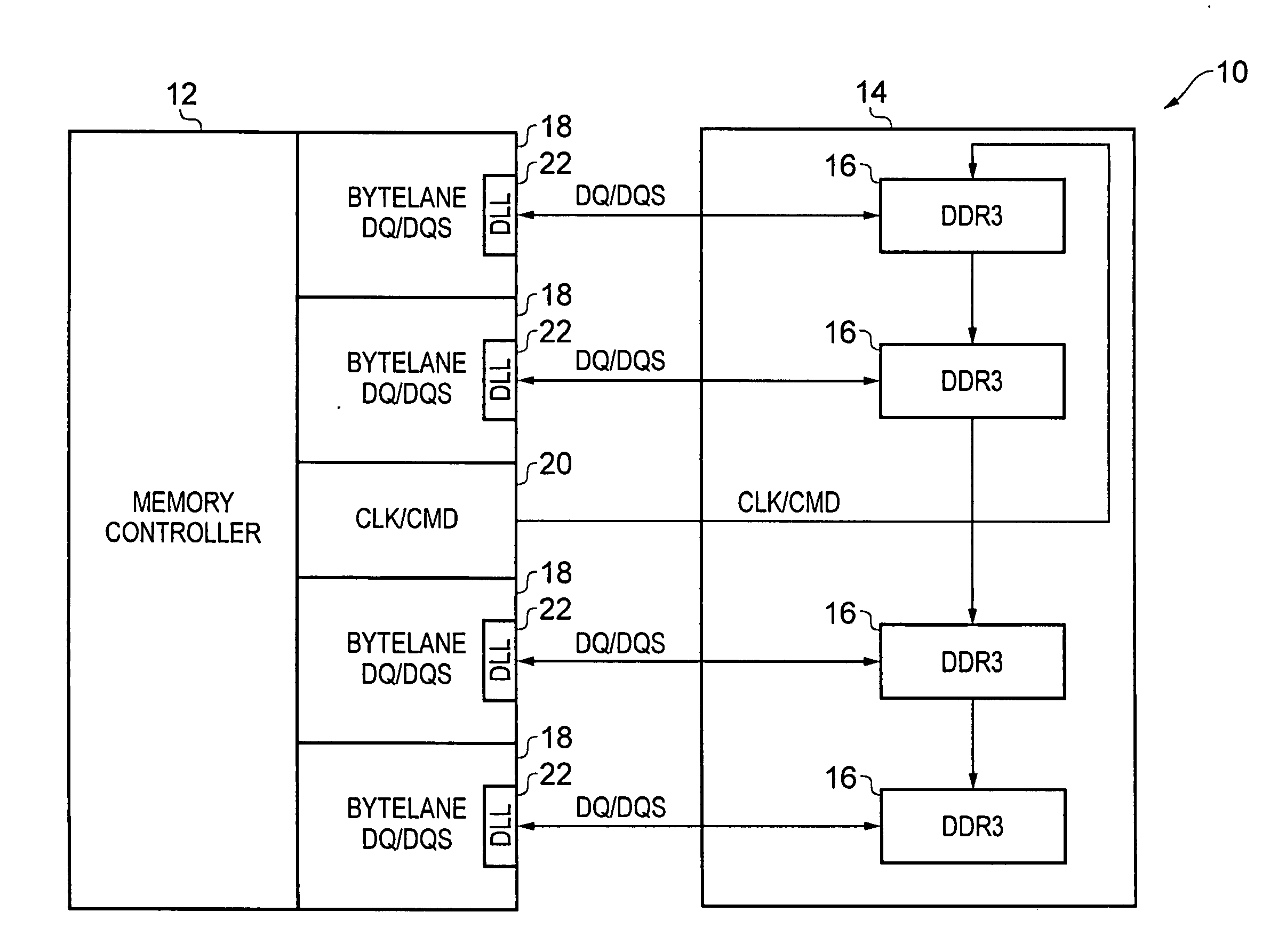
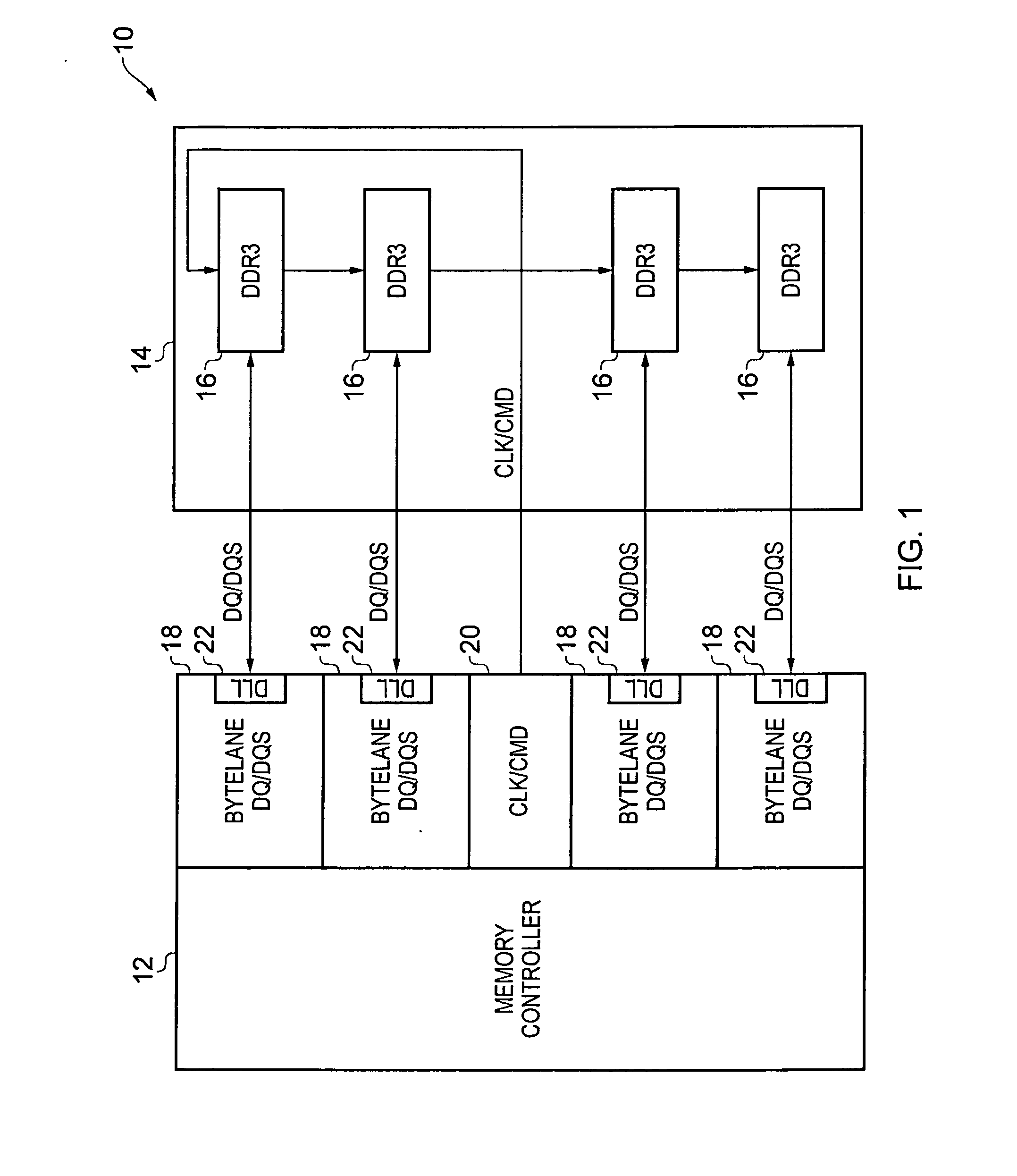
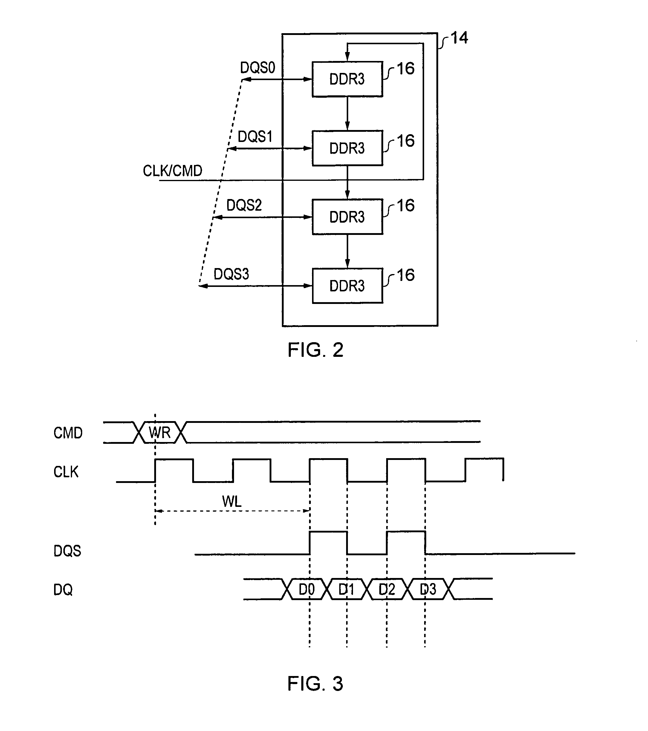
[0070]FIG. 1 schematically illustrates a DDR memory system 10, which generally comprises a memory controller integrated circuit 12 and a memory module integrated circuit 14. The memory module integrated circuit 14 comprises four DDR3 modules 16, each of which may be accessed in parallel by its own dedicated bytelane 18 provided as part of the memory controller integrated circuit 12. The memory controller integrated circuit 12 further comprises a clock / command (CLK / CMD) module 20 which is configured to transmit clock and command signals to the DDR3 modules 16. In the illustrated embodiment shown in FIG. 1, the CLK / CMD signals are transmitted between the DDR3 modules in a “fly-by” configuration to improve signal integrity (avoiding the reflections associated with a branching topology). Accordingly, the memory controller 12 can cause data to be read from one of the DDR3 modules 16 by issuing appropriate command (CMD) signals via the CLK / CMD path (in association with the clock signal CL...


PUM


Abstract

A method of aligning a clock signal and a data strobe signal in a system comprising a memory controller and a memory, and a corresponding memory system are provided. The method comprising the steps of: putting the memory into a write levelling mode; incrementing an alignment delay applied to the data strobe signal until a transition point occurs at which a response of the memory to issuance of the data strobe signal transitions to an inverse state; performing an oversampling of the response of the memory over a selected interval following said transition point; repeating the steps of incrementing and performing an oversampling until, for a selected alignment delay, a majority of results of the oversampling is in the inverse state; performing a cycle alignment detection procedure to determine an identified clock cycle of a plurality of adjacent cycles of the clock signal, the identified clock cycle responsible for the transition point; and applying the selected alignment delay to the data strobe signal and applying a clock cycle selection to a data path in the system to match the identified clock cycle.

Description

BACKGROUND OF THE INVENTION[0001]This application incorporates by reference the subject matter disclosed in each of the concurrently filed applications entitled “An Interface For Controlling The Phase Alignment Of Clock Signals For A Recipient Device” by Gyan Prakash et al (attorney reference no. 550-1573) and “A data signal receiver and method of calibrating a data signal receiver” by Nidhar Kumar et al (attorney reference no. 550-1572).”[0002]1. Field of the Invention[0003]The present invention relates to a method and apparatus for aligning a clock signal and a data strobe signal in a system comprising a memory controller and a memory. More particularly, this invention relates to determining a delay applied to the data strobe signal to align it with the clock signal.[0004]2. Description of the Prior Art[0005]In a memory system comprising a memory controller and a memory, it is known for the memory controller to carry out a write levelling calibration of the memory system during an...

Claims


Application Information

Patent Timeline
Patent Type & Authority Applications(United States)
IPC IPC(8): G11C7/22
CPCG11C7/1066G11C7/1093G11C7/222G11C11/4076G11C11/4093G06F13/1689G11C2207/2254G11C7/22
Inventor KUMAR, NIDHIRPRAKASH, GYANNARLA, CHANDRASHEKAR
Owner ARM LTD
Why Eureka
Try Eureka