Compact and low loss Y-junction for submicron silicon waveguide

a silicon waveguide, compact technology, applied in the direction of optical elements, genetic algorithms, instruments, etc., can solve the problems of not always going in parallel, y-junction is theoretically lossless, and the violation of the y-junction in fabrication,

Active Publication Date: 2014-06-26
NOKIA SOLUTIONS & NETWORKS OY
View PDF10 Cites 27 Cited by
  • Summary
  • Abstract
  • Description
  • Claims
  • Application Information

AI Technical Summary

Problems solved by technology

However, these two advantages do not always go in parallel.
For example, a Y-junction is theoretically lossless, while this is generally not the case due to limited resolution of micro fabrication.
The possible detrimental effects of this violation in fabrication includes peeling off of photoresists, shallower etch in the narrow gap, and voids in subsequent oxide cladding deposition.
All the above degrade device performance and lower yield.
Mach-Zehnder modulators having two such Y-branches readily have more than 2 dB insertion loss in the budget, regardless of other losses from free carrier absorption and on-and-off chip light coupling, making them less competitive to their III-V counterparts.
In addition, complicated integrated optical circuits cannot be built on such lossy components.
Moreover, the abrupt waveguide discontinuity causes light scattering and back-reflection.
However, a Y-junction with low excess loss, low wavelength sensitivity, small footprint, and dimensions clearly within the typical design rules of a modern CMOS photonics process has remained elusive.
Usually these devices have large insertion loss, large footprint, high wavelength sensitivity or low compatibility with CMOS fabrication methods.

Method used


Image

  • Compact and low loss Y-junction for submicron silicon waveguide
  • Compact and low loss Y-junction for submicron silicon waveguide
  • Compact and low loss Y-junction for submicron silicon waveguide

Examples


Embodiment Construction

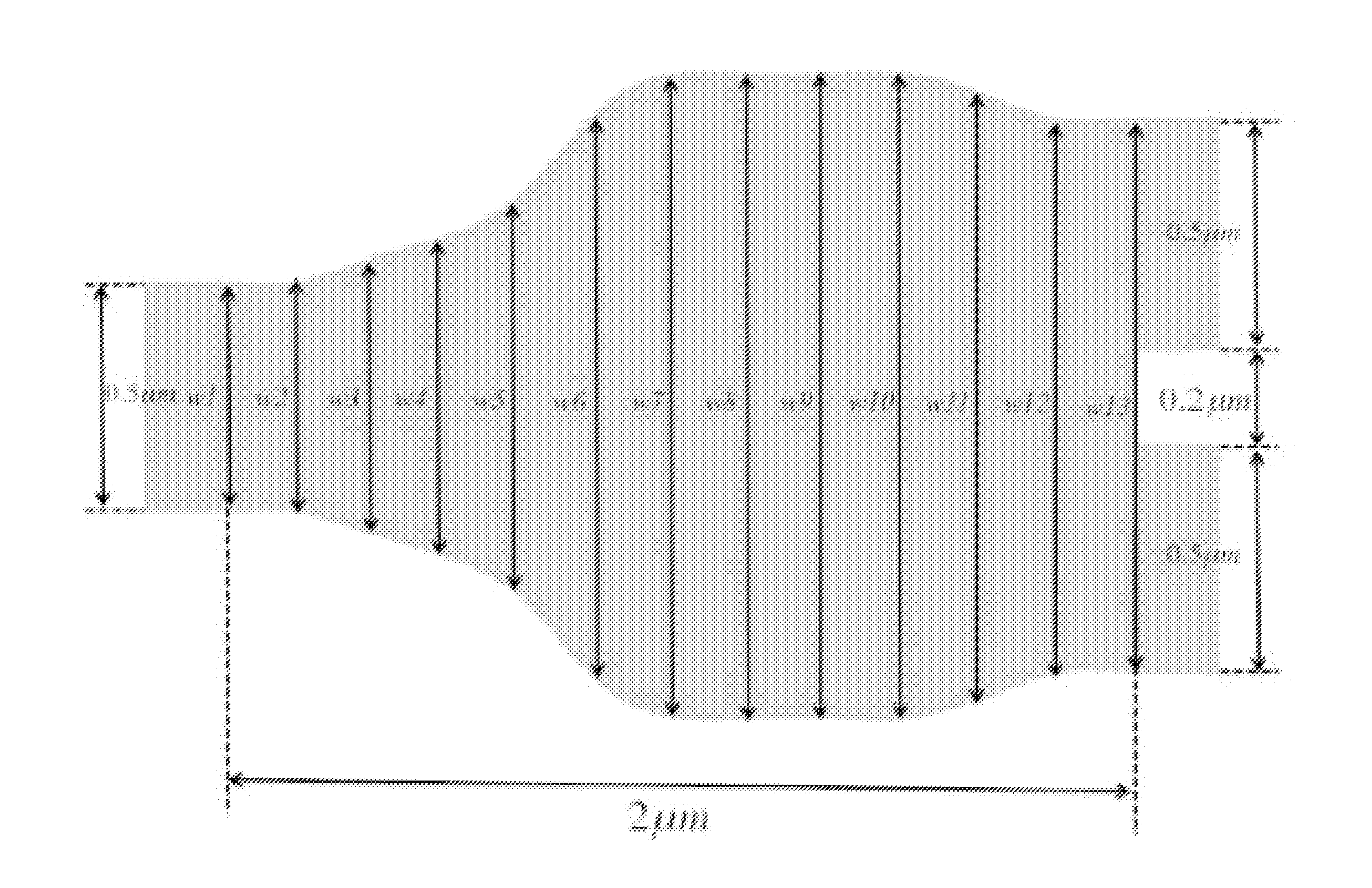
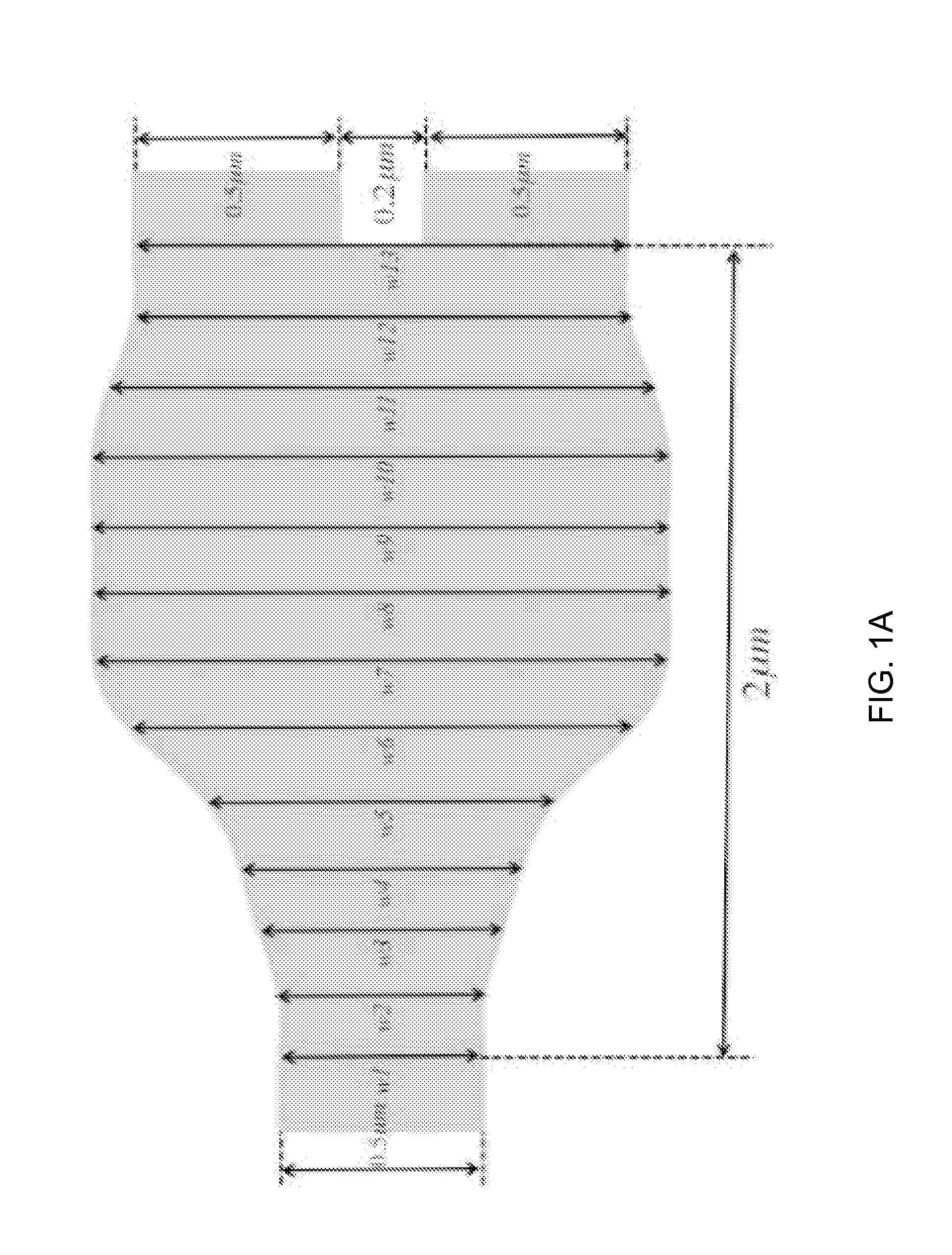
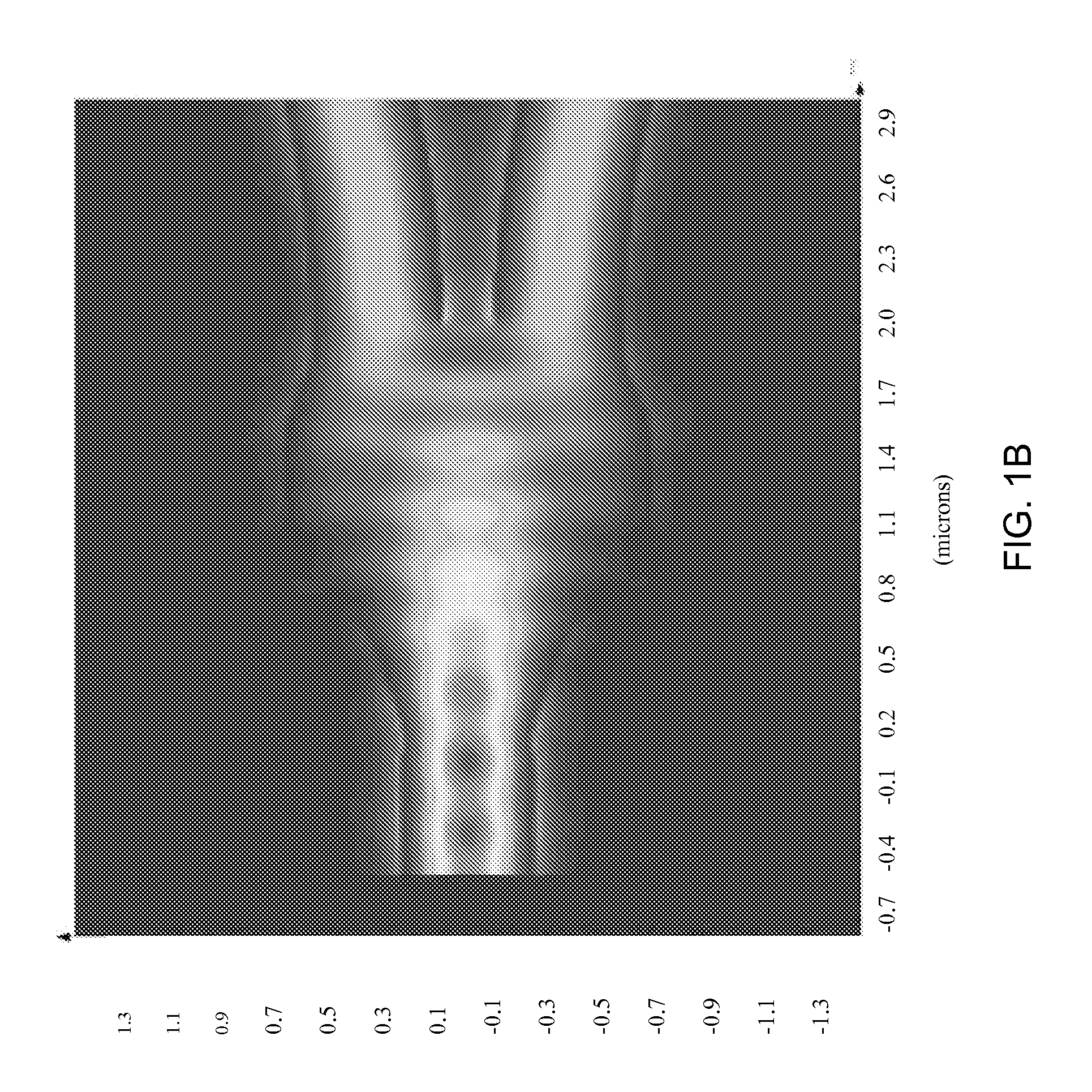
[0029]We have designed a compact, low-loss and wavelength insensitive Y-junction for submicron silicon waveguide using FDTD and particle swarm optimization (PSO), and fabricated the device in a 248 nm CMOS line. We have measured an average insertion loss of 0.28±0.02 dB across an 8-inch wafer. The device footprint is less than 1.2 μm×2 μm, orders of magnitude smaller than MMI and directional couplers. The function of the invention is to provide a 1×2 power splitter for submicron silicon waveguides.

[0030]Our device has very low loss, small footprint, low wavelength sensitivity and was successfully fabricated by 248 nm CMOS with good cross-wafer uniformity.

[0031]The device can be part of a more complicated optoelectronic device, such as a Mach-Zehnder modulator, or a basic building block of integrated silicon photonic circuit.

[0032]The device can be a useful component of the process design kit (PDK) of a silicon photonics foundry. Companies commercializing silicon photonics technology...


PUM


Abstract

A compact, low-loss and wavelength insensitive Y-junction for submicron silicon waveguides. The design was performed using FDTD and particle swarm optimization (PSO). The device was fabricated in a 248 nm CMOS line. Measured average insertion loss is 0.28±0.02 dB across an 8-inch wafer. The device footprint is less than 1.2 μm×2 μm, orders of magnitude smaller than MMI and directional couplers.

Description

CROSS-REFERENCE TO RELATED APPLICATIONS[0001]This application claims priority to and the benefit of co-pending U.S. provisional patent application Ser. No. 61 / 731,502, filed Nov. 30, 2012, which application is incorporated herein by reference in its entirety.STATEMENT REGARDING FEDERALLY FUNDED RESEARCH OR DEVELOPMENT[0002]This invention was made with government support under Grant No FA9550-10-1-0053 awarded by the Air Force Office of Scientific Research (AFOSR). The government has certain rights in the invention.FIELD OF THE INVENTION[0003]The invention relates to optical waveguide components in general and particularly to a Y-junction for use with submicron silicon waveguides.BACKGROUND OF THE INVENTION[0004]The last decade witnessed series of break-throughs in silicon photonics. Key components such as the electrically pumped laser (see, for example, R. Camacho-Aguilera, et al, “An electrically pumped germanium laser,” Opt. Express 20, 11316-11320 (2012)), the high-speed modulato...

Claims


Application Information

Patent Timeline
Patent Type & Authority Applications(United States)
IPC IPC(8): G02B6/28
CPCG02B6/2808G02B6/1223G02B2006/1215G02B2006/12061G02B6/125G06F30/20G06F30/23G06F30/394G02B6/107G02B27/0012G02B6/1228G02B2006/12038G06N3/126
Inventor ZHANG, YIYANG, SHUYUBAEHR-JONES, TOM
Owner NOKIA SOLUTIONS & NETWORKS OY
Why Eureka
Try Eureka