

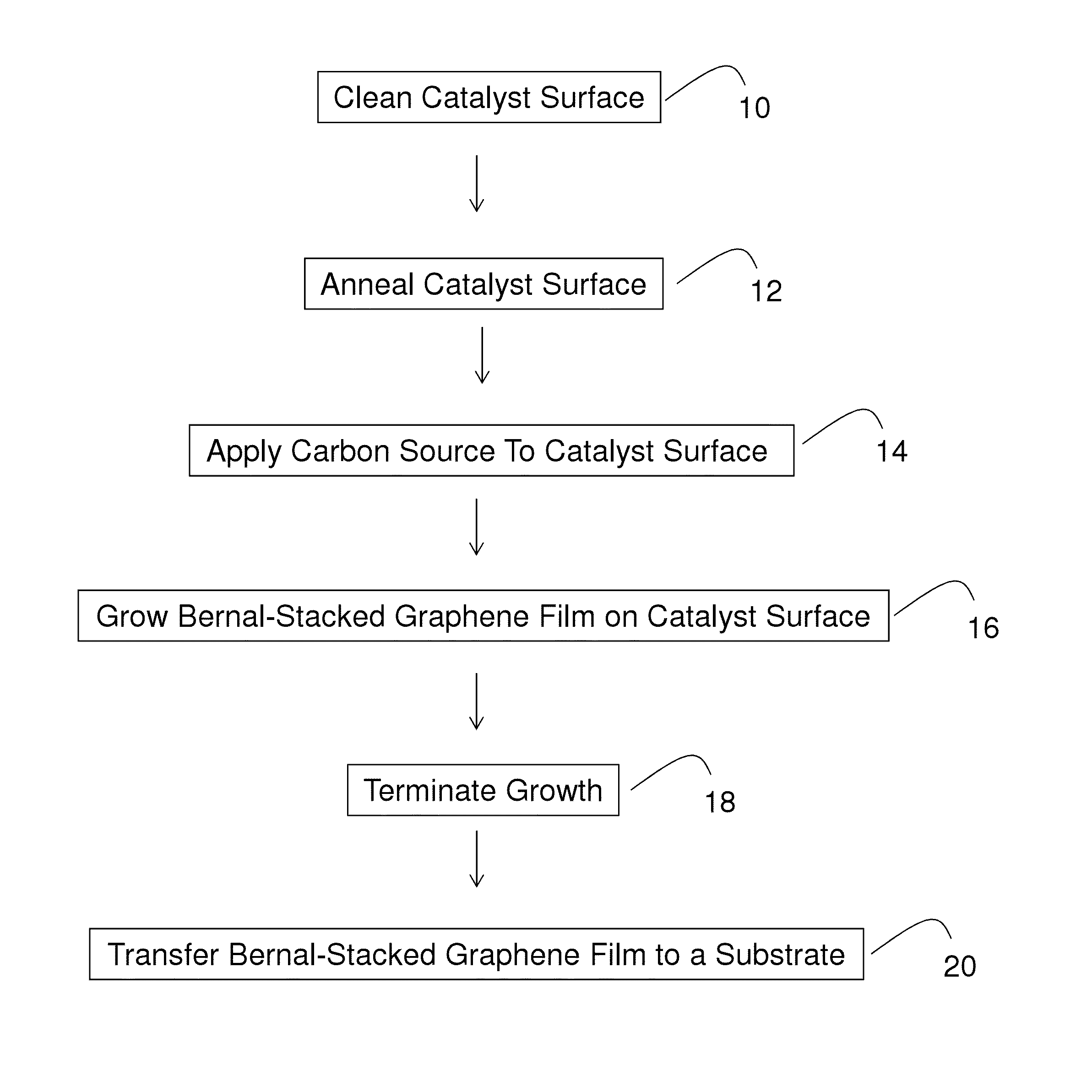
Bernal-stacked graphene layers and methods of making the same
a graphene layer and graphene layer technology, applied in the field of controllable forming bernal-stacked graphene layers, can solve the problems of scalability, uniformity, and the inability to control the number of formed bernal-stacked graphene layers
- Summary
- Abstract
- Description
- Claims
- Application Information
AI Technical Summary
Benefits of technology
Problems solved by technology
Method used
Image

Examples
example 1
Preparation of Large-Area Bernal-Stacked Bi-, Tri-, and Tetralayer Graphene
[0091]In this Example, Applicants demonstrate that large-area uniform Bernal-stacked bi-, tri-, and tetralayer graphene films were successfully synthesized on a Cu surface in selective growth windows, with a finely tuned total pressure and CH4 / H2 gas ratio. Based on the analyses obtained, the growth mechanism is not an independent homoexpitaxial layer-by-layer growth, but most likely a simultaneous-seeding and self-limiting process.
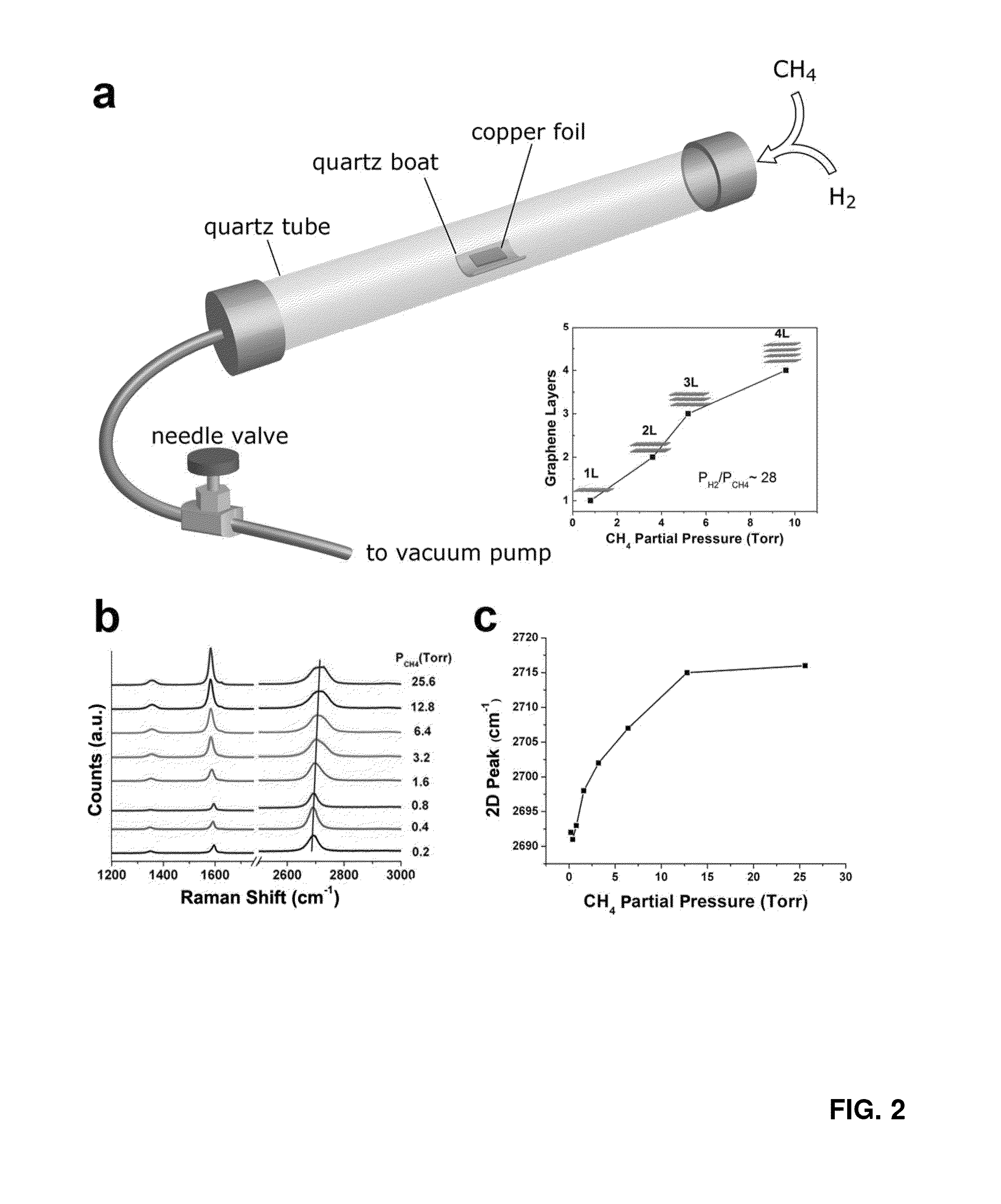
[0092]In this Example, Applicants demonstrate consistent chemical vapor deposition (CVD) growth windows for large-area Bernal-stacked bi-, tri-, or tetralayer graphene on Cu surfaces. Without being bound by theory, Applicants have demonstrated that parameters that could affect the thickness of graphene growth include the pressure in the system, gas flow rate, growth pressure (the partial pressure of both the growth gas and the carrier gas), growth temperature, and cooling rate. Bas...
example 1.1
CVD Growth
[0107]In a 48-inch-long fused quartz tube (22-mm ID, 25-mm OD, Technical Glass Products) heated in a furnace, graphene films were grown on a ˜1 in2 copper foil mounted on a boat-shaped quartz holder with a magnet affixed at one end to facilitate insertion and removal (the magnet never enters to hot-zone of the oven). With the furnace heated to 1000° C. and tube under vacuum (2 (ultra-high purity grade, 99.999% from Matheson) was introduced at 300 sccm and the H2 pressure was controlled with a needle valve (FIG. 2A) to a specified value. The copper foil was then annealed for 10 min by sliding the holder containing the copper to the center of the furnace. In the presence of the pressure-controlled H2, filtered methane (chemical purity grade, 99.0%, Matheson) was opened at 10±1 sccm for a growth time of 15 min after which the holder was removed from the furnace area of the tube to cool under H2. The copper foil was 25 μm thick and 99.8% grade, purchased from Alfa Aesar.
example 1.2
Transfer
[0108]Graphene was formed on both sides of the Cu foil. In order to protect the graphene layers during Cu etching, a poly(methyl methacrylate) (PMMA) solution (950 PMMA A 4, MicroChem) was spin-coated (at 2500 rpm for 1 min) on the top of the graphene-coated copper foil twice and baked at 70° C. for ˜30 min in a vacuum oven or on a hot plate. Marble's reagent was used as an aqueous etchant solution, comprising 15.6 g CuSO4.5H2O (Aldrich), 45 mL deionized H2O, and 50 mL conc. HCl (Aldrich). The PMMA-graphene-Cu assembly was etched for a few min after which the Cu foil was removed from the Marble's reagent and dipped in water several times and wiped on a Kim wipe to completely remove the unprotected graphene on bottom of the Cu foil so that its residue did not merge with the top graphene. The remaining Cu was etched, leaving the PMMA-protected graphene that had been on top of the Cu foil floating on the etchant. The film was floated on deionized water and subsequently transfer...
PUM
| Property | Measurement | Unit |
|---|---|---|
| pressure | aaaaa | aaaaa |
| surface area | aaaaa | aaaaa |
| temperatures | aaaaa | aaaaa |
Abstract
Description
Claims
Application Information