Avalanche photodiode-type semiconductor structure with low response time and process for producing such a structure

Active Publication Date: 2014-07-03
COMMISSARIAT A LENERGIE ATOMIQUE ET AUX ENERGIES ALTERNATIVES
View PDF1 Cites 3 Cited by
  • Summary
  • Abstract
  • Description
  • Claims
  • Application Information

AI Technical Summary

Benefits of technology

The patent describes a method to create an avalanche photodiode structure with a first zone made of mercury-cadmium telluride that has a varying concentration of cadmium. This helps to reduce the diffusion of cadmium during the activation anneal and ensures a low series resistance. The structure also has a good conduction over the entire thickness of the first zone, which helps to accelerate the diffusion of carriers and reduce the response time of the structure. The use of a low concentration of doping element in the first zone also limits the risk of diffusion of cadmium. Overall, this method produces an improved avalanche photodiode structure with better performance and reliability.

Problems solved by technology

Nevertheless, even if such structures have improved characteristics with respect to structures made of a different material, they have the disadvantage of not enabling, in a conventional configuration, a variation in the forbidden energy gap in the first semiconductor zone, which could, for example, enable the response time of the structure to be improved.

Method used


Image

  • Avalanche photodiode-type semiconductor structure with low response time and process for producing such a structure
  • Avalanche photodiode-type semiconductor structure with low response time and process for producing such a structure
  • Avalanche photodiode-type semiconductor structure with low response time and process for producing such a structure

Examples


first embodiment

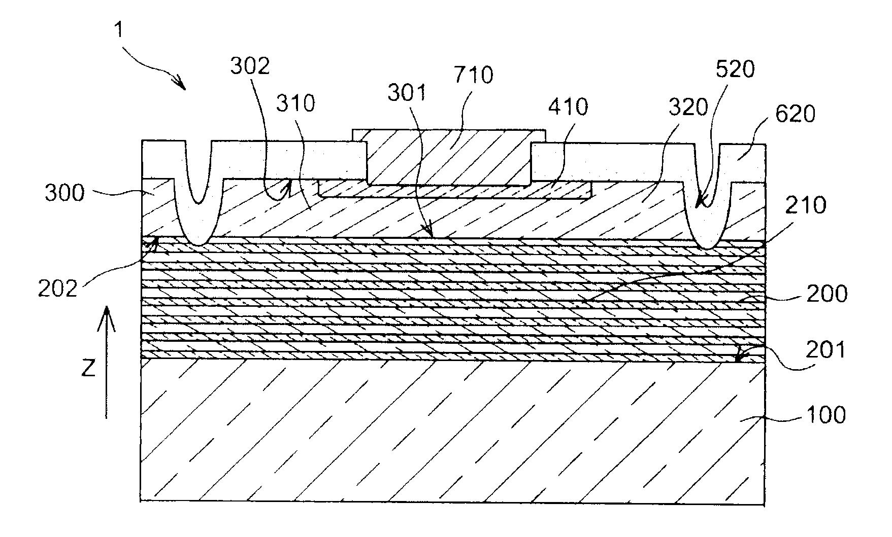
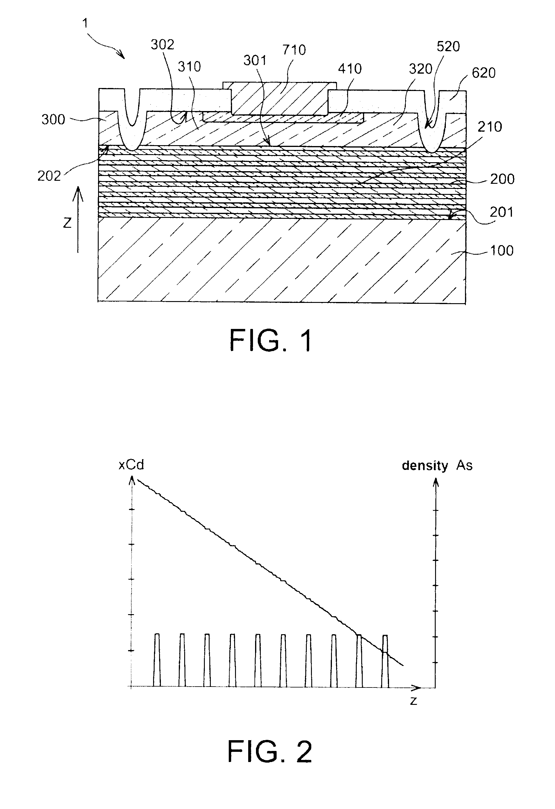
[0049]FIG. 1 shows a cross-section view of a structure according to the invention,

[0050]FIG. 2 shows a graph of the variations in cadmium and arsenic concentrations in a first semiconductor zone of a first structure as shown in FIG. 1,

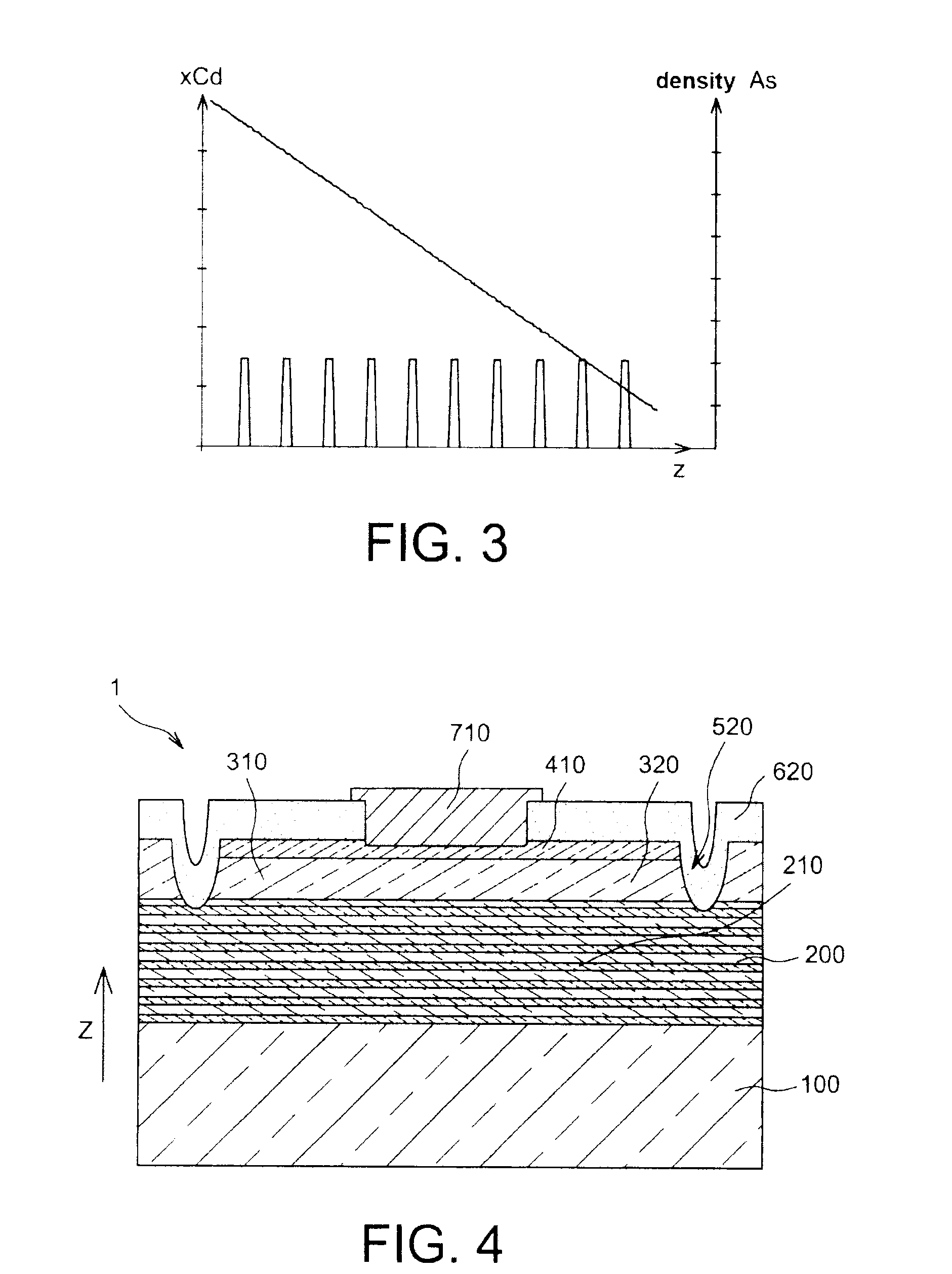
[0051]FIG. 3 shows a graph of the variations in cadmium and arsenic concentrations in the first semiconductor zone of a structure as shown in FIG. 1 during its production before the arsenic activation step,

second embodiment

[0052]FIG. 4 shows a cross-section view of a structure according to the invention in which the structure comprises a third semiconductor zone that extends over the entire width of the second semiconductor zone,

third embodiment

[0053]FIG. 5 shows a cross-section view of a structure according to the invention in which the structure comprises an adaptation layer,


PUM


Abstract

The invention relates to an avalanche photodiode-type semiconductor structure (1) intended to receive electromagnetic radiation in a given wavelength. The structure comprises a first semiconductor zone (210) with a first type of conductivity with a first longitudinal face (201), said first zone (210) being made of mercury-cadmium telluride of the CdxHg1-xTe type with a cadmium proportion x that is varied. The structure (1) also comprises at least one second semiconductor zone (310) in contact with the first zone (210), and a third semiconductor zone (410) in contact with the second zone (310). The first zone (210) comprises a doping element, such as arsenic, of which the concentration is varied alternately in a direction substantially perpendicular to the first longitudinal face (201) between a so-called low concentration and a so-called high concentration. The invention also relates to a process for producing a structure (1) according to the invention.

Description

TECHNICAL FIELD[0001]The invention relates to the field of light measurement and detection devices.[0002]In recent years, the application of microelectronic production methods to direct gap semiconductor materials, such as gallium arsenide and indium phosphide, have made it possible to improve the performance of optoelectronic structures.[0003]Thus, among these optoelectronic structures, the application of these technologies to the current avalanche photodiode technologies has made it possible to reduce their dark current, thus improving their sensitivity, and their response time. In spite of the low response time of these structures, research aimed at reducing the response time of avalanche photodiodes remains a current problem.[0004]The invention therefore more specifically relates to an avalanche photodiode-type semiconductor structure with a low response time and to a process for producing such a structure.PRIOR ART[0005]Recent research studies on avalanche photodiodes based on ...

Claims


Application Information

Patent Timeline
IPC IPC(8): H01L31/0296H01L31/107H01L31/18
CPCH01L31/02966H01L31/1832H01L31/107H01L31/1032H01L31/1075
Inventor ROTHMAN, JOHAN
Owner COMMISSARIAT A LENERGIE ATOMIQUE ET AUX ENERGIES ALTERNATIVES
Why Eureka
Try Eureka