

Power semiconductor device
a technology of power semiconductor and semiconductor chip, which is applied in the direction of semiconductor/solid-state device details, pulse technique, electronic switching, etc., can solve the problems of difficult to reduce the chip size of the mosfet and the size reduction of the entire device, and achieve the effect of reducing the size of the entire power semiconductor devi
- Summary
- Abstract
- Description
- Claims
- Application Information
AI Technical Summary
Benefits of technology
Problems solved by technology
Method used
Image

Examples
embodiment
Preferred Embodiment
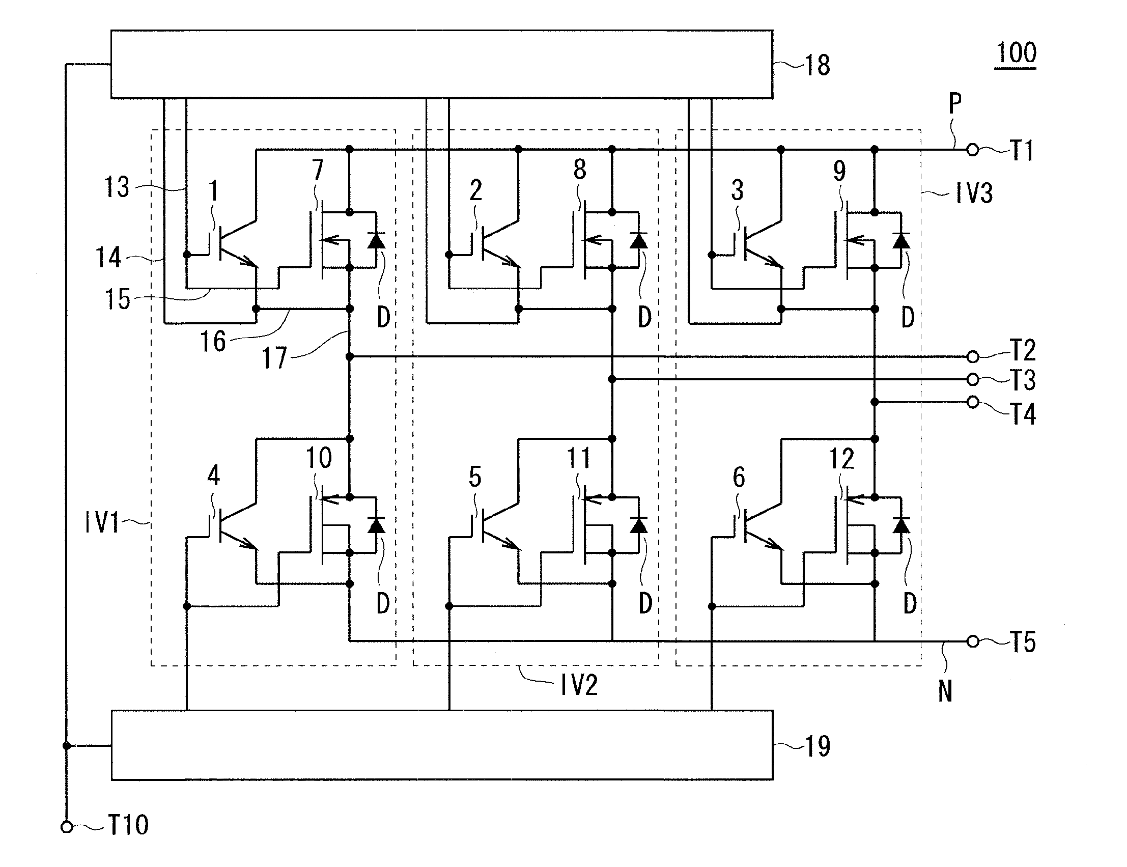
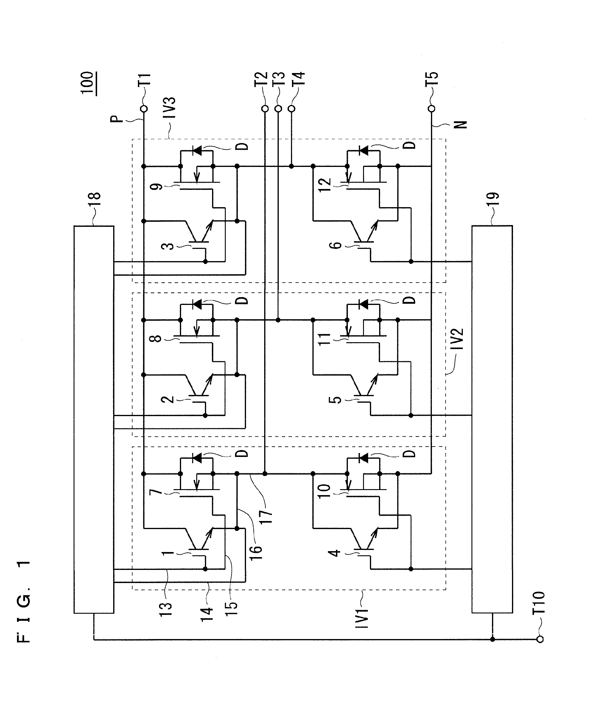
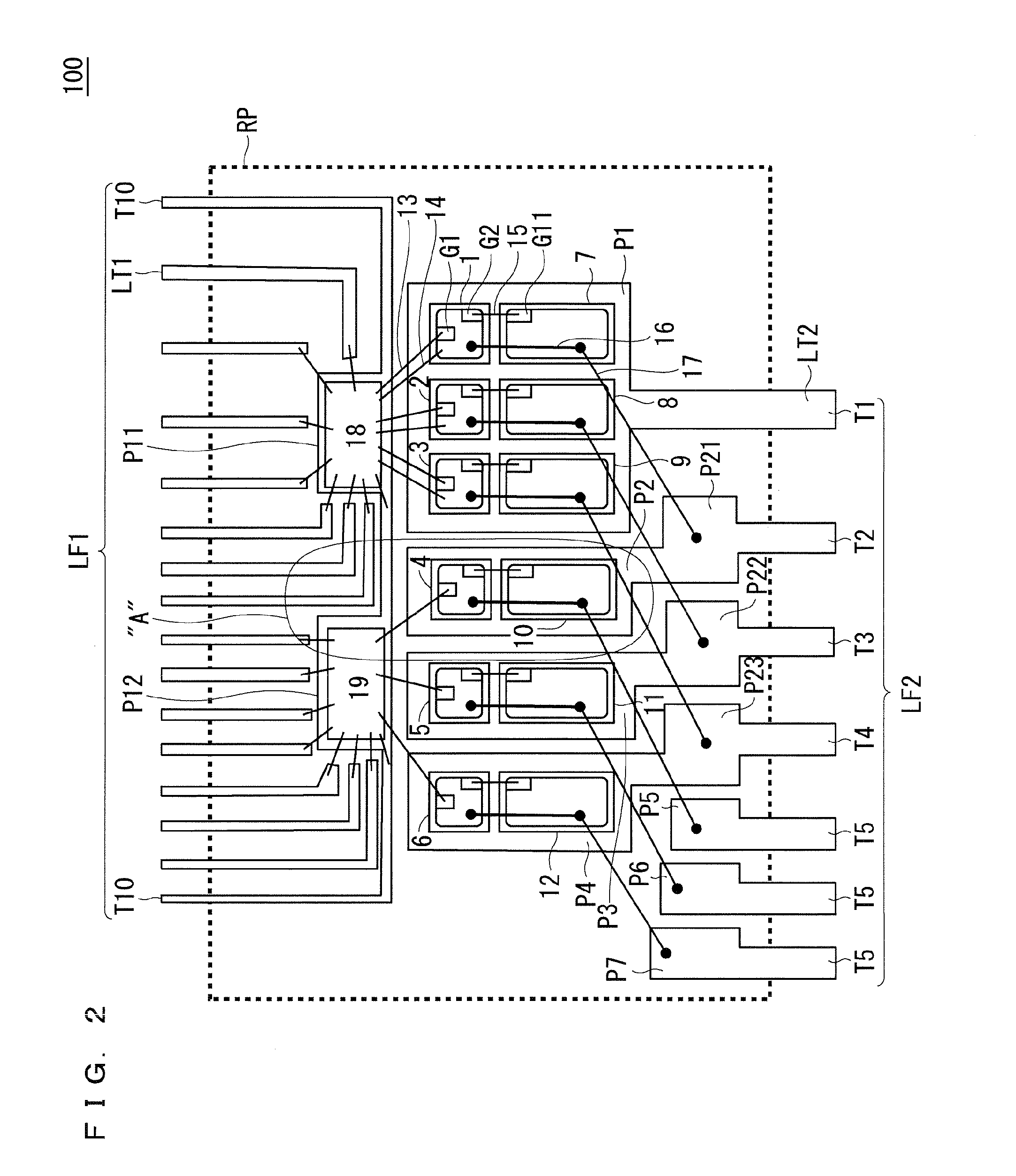
[0030]FIG. 1 shows the circuit structure of a three-phase inverter module 100 according to a preferred embodiment of a power semiconductor device of the present invention.
[0031]The three-phase inverter module 100 of FIG. 1 is composed of three inverters IV1 to IV3.
[0032]The inverter IV1 includes MOSFETs (MOS field effect transistors) 7 and 10 connected in series between a power source line P connected to a terminal T1 to receive a power source voltage and a power source line N connected to a terminal T5 to receive a reference voltage, and IGBTs (insulated gate bipolar transistors) 1 and 4 connected in parallel to the MOSFETs 7 and 10 respectively. The respective sources and the respective drains of the MOSFETs 7 and 10 are connected in common to a terminal T2. The IGBT 1 and the MOSFET 7 are high-potential side switching devices which form a high-potential side switching part. The IGBT 4 and the MOSFET 10 are low-potential side switching devices which form a low-...
PUM
| Property | Measurement | Unit |
|---|---|---|
| diameter | aaaaa | aaaaa |
| length | aaaaa | aaaaa |
| resistance | aaaaa | aaaaa |
Abstract
Description
Claims
Application Information