Semiconductor device

a technology of semiconductors and devices, applied in the direction of semiconductor devices, basic electric elements, electrical equipment, etc., can solve the problems of device breakdown and loss, and achieve the effect of improving the ability to reverse the effect of recovery

Active Publication Date: 2014-07-17
FUJI ELECTRIC CO LTD
View PDF22 Cites 33 Cited by
  • Summary
  • Abstract
  • Description
  • Claims
  • Application Information

AI Technical Summary

Benefits of technology

[0020]According to the aforementioned configuration of the invention, a p-buffer layer (second conductivity-type layer) is provided selectively inside an n-buffer layer (first conductivity-type layer) in an edge termination region so that electrons injected into a second parallel pn structure from an n+ drain layer (low-resistivity layer) on the back side can be restrained. In accordance with this, holes injected into the second parallel pn str...

Problems solved by technology

On the contrary, in the semiconductor device with high breakdown voltage, the n− drift layer is so thick that on-resistance becomes high enough increase the loss.
As a result, there...

Method used


Image

  • Semiconductor device
  • Semiconductor device
  • Semiconductor device

Examples


embodiment 1

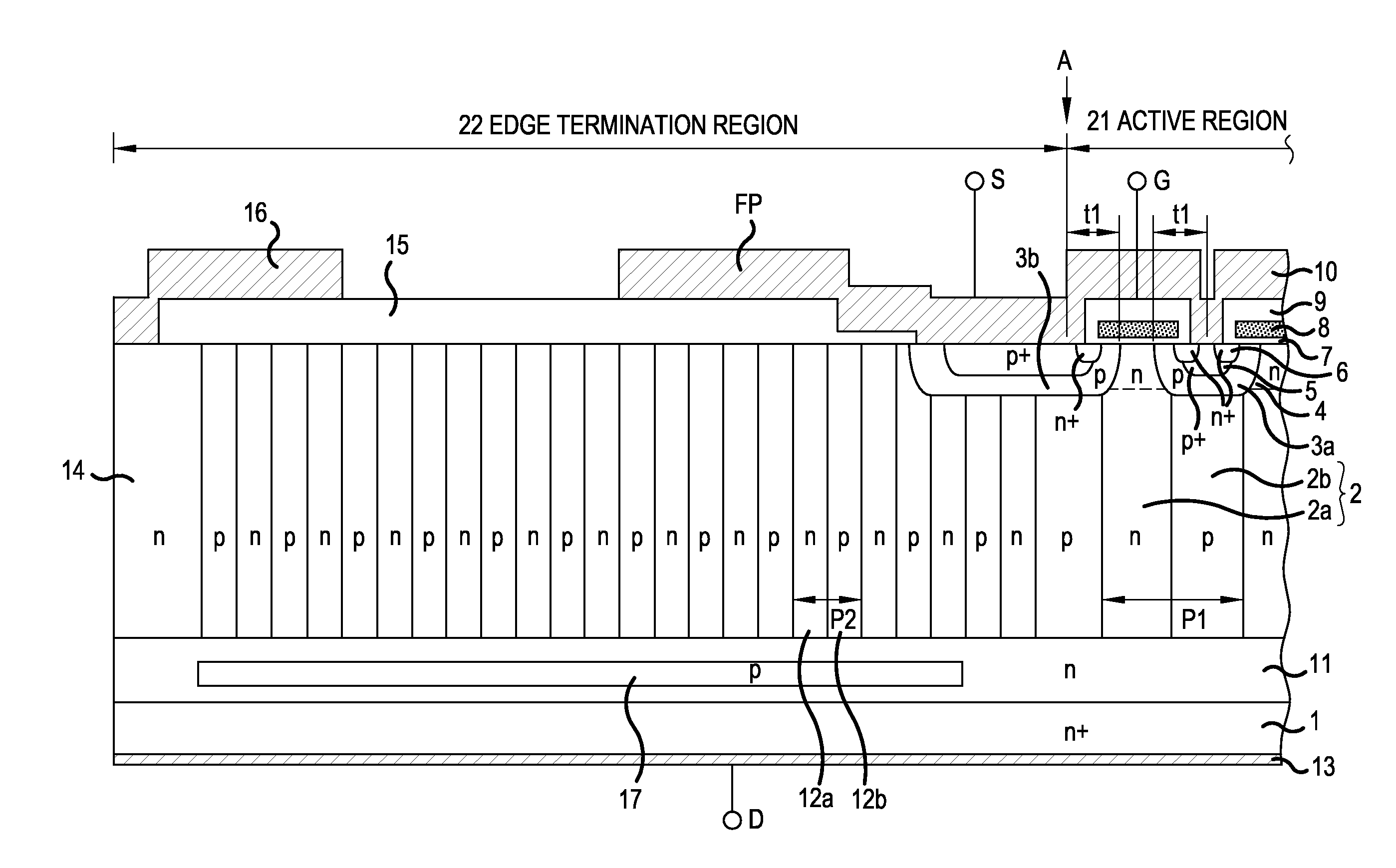
[0042]As for the structure of a semiconductor device according to Embodiment 1, an n-channel vertical MOSFET with a planar gate structure will be described by way of example. FIG. 1 is a cross sectional view of the semiconductor device according to Embodiment 1. The semiconductor device according to Embodiment 1 shown in FIG. 1 is a superjunction MOSFET which is formed so that n-buffer layer (first conductivity-type layer) 11 and drain drift portion (vertical drift portion) 2 with a first parallel pn structure are laminated sequentially on low resistivity n+ drain layer (low-resistivity layer) 1 with which drain electrode 13 on the back side of a substrate makes ohmic contact. The substrate is an epitaxial substrate which will be described later.

[0043]P-base regions 3a with high impurity concentration serving as active region 21 are provided selectively on the front side (an opposite side to the n-buffer layer 11 side) surface layer of drain drift portion 2. P+ contact region 5 with...

embodiment 2

[0065]The structure of a superjunction semiconductor device according to Embodiment 2 will be described. FIG. 7 is a cross sectional view showing the structure of the semiconductor device according to Embodiment 2. The superjunction semiconductor device according to Embodiment 2 is different from the superjunction semiconductor device according to Embodiment 1 in the following two points. The first different point is that n-type bulk region 42 consecutive to the first parallel pn structure is provided in place of the second parallel pn structure and p-type RESURF region 43 is provided in a front side surface layer of n-type bulk region 42. The second different point is that an outer end portion of p-buffer layer 41 is extended up to the outer periphery (side surface) of edge termination region 22.

[0066]N-type bulk region 42 is a region between the first parallel pn structure provided to extend from active region 21 to edge termination region 22, and n-type channel stopper region 14 ...

embodiment 3

[0071]The structure of a superjunction semiconductor device according to Embodiment 3 will be described. FIG. 12 is a cross sectional view showing the structure of the semiconductor device according to Embodiment 3. The superjunction semiconductor device according to Embodiment 3 is different from the superjunction semiconductor device according to Embodiment 1 in the following two points. The first different point is that the depth of a parallel pn structure in device peripheral portion 22 becomes shallower as it goes toward the outer periphery. The second different point is that the parallel pn structure in edge termination region 22 is separated from the p-buffer layer by n-type region (first conductivity-type region) 64 formed in a region where the parallel pn structure in edge termination region 22 becomes shallower.

[0072]A third parallel pn structure is provided in edge termination region 22 so as to be consecutive to the second parallel pn structure and outside the second par...


PUM


Abstract

A superjunction semiconductor device is disclosed in which the tradeoff relationship between on-resistance and breakdown voltage is improved greatly so that reverse recovery capability is improved. A drain drift portion substantially corresponds to a portion just under p-base regions serving as an active region and forms a first parallel pn structure in which a first n-type region and a first p-type region are joined to each other alternately and repeatedly. A drain drift portion is surrounded by edge termination region including a second parallel pn structure. Edge termination region is formed such that second n-type and p-type regions oriented consecutively to the first parallel pn structure of the drain drift portion are joined to each other alternately and repeatedly. N-buffer layer is provided between first and second parallel pn structures and n+ drain layer. P-buffer layer is provided selectively inside n-buffer layer in edge termination region.

Description

BACKGROUND OF THE INVENTION[0001]A. Field of the Invention[0002]This invention relates to a semiconductor device.[0003]B. Description of the Related Art[0004]Generally, semiconductor devices are classified into horizontal semiconductor devices having electrodes on one side and vertical semiconductor devices having electrodes on opposite sides. In a vertical semiconductor device, a direction in which a drift current flows in the ON state coincides with a direction in which a depletion layer spreads due to a reverse bias voltage in the OFF state. For example, in an n-channel vertical MOSFET (Metal Oxide Semiconductor Field Effect Transistor) with an ordinary planar gate structure, a high resistivity n− drift layer portion operates as a region where a drift current flows vertically in the ON state. Accordingly, drift resistance is reduced when the current path of the n− drift layer is shortened. It is therefore possible to obtain an effect that substantial on-resistance of the MOSFET c...

Claims


Application Information

Patent Timeline
IPC IPC(8): H01L29/78
CPCH01L29/7811H01L29/063H01L29/78H01L29/402H01L29/41741H01L29/66712H01L29/0623H01L29/0634H01L29/0638H01L29/0615H01L29/1095
Inventor ONISHI
Owner FUJI ELECTRIC CO LTD
Why Eureka
Try Eureka