Isolation structure of high-voltage driving circuit

a driving circuit and isolation structure technology, applied in the direction of basic electric elements, electrical equipment, semiconductor devices, etc., can solve the problems of partial breakdown phenomenon, resistance to voltage and leak current,

Active Publication Date: 2014-07-24
SOUTHEAST UNIV
View PDF2 Cites 10 Cited by
  • Summary
  • Abstract
  • Description
  • Claims
  • Application Information

AI Technical Summary

Benefits of technology

[0010](3) The present invention is compatible with the existing proce

Problems solved by technology

However, withstand voltage and leak current are two major challenges in the design and technique of isolation structures.
However, when the high-voltage region is connected to high voltage, the P-type junction isolation region near the

Method used


Image

  • Isolation structure of high-voltage driving circuit
  • Isolation structure of high-voltage driving circuit
  • Isolation structure of high-voltage driving circuit

Examples


embodiment 1

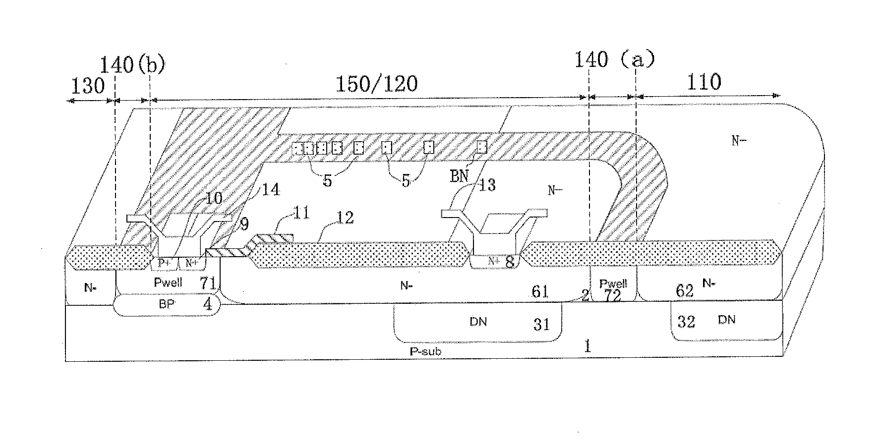
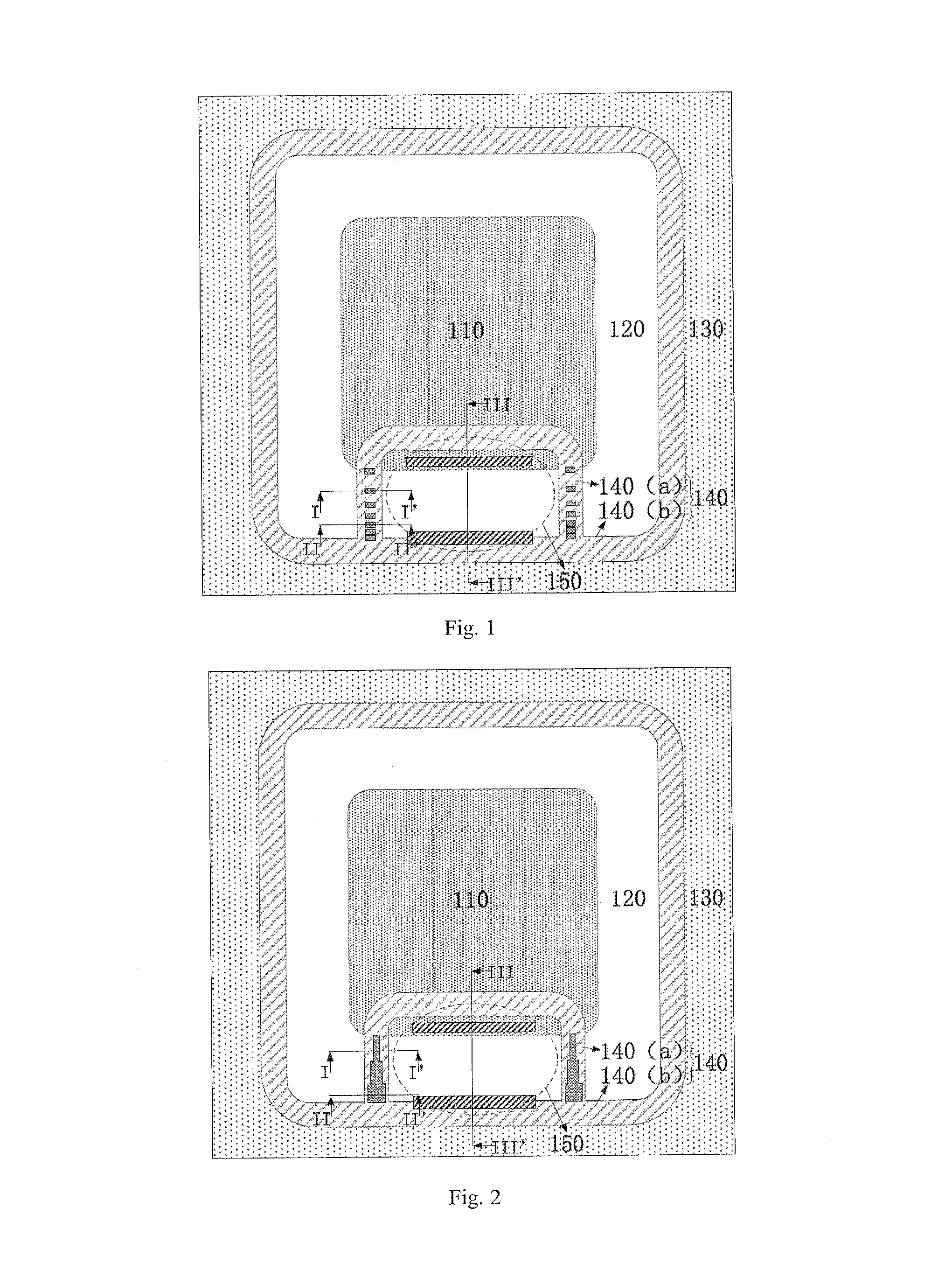
[0021]An isolation structure of high-voltage driving circuit, comprising: a P-type substrate 1; a P-type epitaxial layer 2 arranged on the P-type substrate 1; a low-voltage region 130 and a high-voltage region 110 arranged on the P-type epitaxial layer 2; a HV-LV junction terminal region 120 arranged between the low-voltage region 130 and the high-voltage region 110; a first P-type junction isolation region 140a arranged between the HV-LV junction terminal region 120 and the low-voltage region 130, said first P-type junction isolation region 140a being composed of a P-type buried layer 4 and a first P-type well 71; a second P-type junction isolation region 140b arranged in the interior zone of the first P-type junction isolation region 140a and working with the first P-type junction isolation region 140a to enclose an isolated region; a high-voltage insulated gate field effect transistor (IGFET) 150 arranged in the isolated region and utilizing the HV-LV junction terminal region 120...

embodiment 2

[0022]An isolation structure of high-voltage driving circuit, comprising: a P-type substrate 1; a P-type epitaxial layer 2 arranged on the P-type substrate 1; a low-voltage region 130 and a high-voltage region 110 arranged on the P-type epitaxial layer 2; a HV-LV junction terminal region 120 arranged between the low-voltage region 130 and the high-voltage region 110; a first P-type junction isolation region 140a arranged between the HV-LV junction terminal region 120 and the low-voltage region 130, said first P-type junction isolation region 140a being composed of a P-type buried layer 4 and a first P-type well 71; a second P-type junction isolation region 140b arranged in the interior zone of the first P-type junction isolation region 140a and working with the first P-type junction isolation region 140a to enclose an isolated region; a high-voltage insulated gate field effect transistor (IGFET) 150 arranged in the isolated region and utilizing the HV-LV junction terminal region 120...

embodiment 3

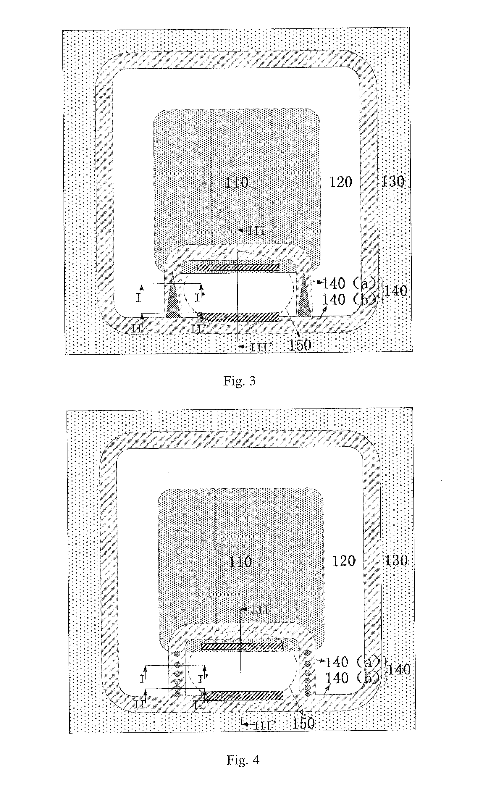
[0023]An isolation structure of high-voltage driving circuit, comprising: a P-type substrate 1; a P-type epitaxial layer 2 arranged on the P-type substrate 1; a low-voltage region 130 and a high-voltage region 110 arranged on the P-type epitaxial layer 2; a HV-LV junction terminal region 120 arranged between the low-voltage region 130 and the high-voltage region 110; a first P-type junction isolation region 140a arranged between the HV-LV junction terminal region 120 and the low-voltage region 130, said first P-type junction isolation region 140a being composed of a P-type buried layer 4 and a first P-type well 71; a second P-type junction isolation region 140b arranged in the interior zone of the first P-type junction isolation region 140a and working with the first P-type junction isolation region 140a to enclose an isolated region; a high-voltage insulated gate field effect transistor (IGFET) 150 arranged in the isolated region and utilizing the HV-LV junction terminal region 120...


PUM


Abstract

An isolation structure of a high-voltage driving circuit includes a P-type substrate and a P-type epitaxial layer; a high voltage area, a low voltage area and a high and low voltage junction terminal area are arranged on the P-type epitaxial layer; a first P-type junction isolation area is arranged between the high and low voltage junction terminal area and the low voltage area, and a high-voltage insulated gate field effect tube is arranged between the high voltage area and the low voltage area; two sides of the high-voltage insulated gate field effect tube and an isolation structure between the high-voltage insulated gate field effect tube and a high side area are formed as a second P-type junction isolation area.

Description

FIELD OF THE INVENTION[0001]The present invention relates to a high-voltage half-bridge gate driving circuit in a high-voltage power integrated circuit, in particular to an isolation structure in an integrated high-voltage driving circuit.BACKGROUND OF THE INVENTION[0002]High-voltage gate driving circuits can be used in various fields, such as motor driving, electronic ballasts for fluorescent lamp, and power management, etc. The level shift circuit in a high-voltage gate driving circuit is a key component of the entire circuit, the electrical performance of high-voltage insulated gate field effect tube LDMOS elements constituting the level shift circuit and the electrical coupling between high-voltage LDMOS elements have influence on the performance of the level shift circuit, and the heavy current and high voltage of source electrode and drain electrode of the high-voltage LDMOS elements may cause a parasitic effect in other areas of the entire integrated circuit and thereby have ...

Claims


Application Information

Patent Timeline
IPC IPC(8): H01L29/06H01L21/8234H01L21/761
CPCH01L21/265H01L21/761H01L21/823481H01L29/0646H01L29/0692H01L29/7835H01L29/0847H01L29/1083
Inventor SHI, LONGXINGQIAN, QINSONGSUN, WEIFENGZHU, JINGHUANG, XIANGUOLU, SHENGLI
Owner SOUTHEAST UNIV
Why Eureka
Try Eureka