Spin transfer MRAM element having a voltage bias control

Active Publication Date: 2014-07-31
GUO YIMIN
View PDF18 Cites 44 Cited by
  • Summary
  • Abstract
  • Description
  • Claims
  • Application Information

AI Technical Summary

Benefits of technology

[0018]An exemplary embodiment includes method of operating a spin-transfer-torque perpendicular magnetoresistive memory including a circuitry coupled to the bit line positioned adjacent to selected ones of the plurality of magnetoresistive memory elements and coupled to the digital line configured to apply an electric field on the anisotropy modification layer through the voltage bias layer and accordingly reduce the perpendicular anisotropy strength in the recording layer for a low write current during a recording process

Problems solved by technology

However, where a MTJ is formed as a device of a perpendicular magnetization type, the materials of the recording layer typically used in an in-plane MTJ for both high MR and low damping constant as required by low write current application normally don't have enough magnetic crystalline anisotropy to achieve thermally stable perpendicular magnetization against its demagnetization field.
Doing so, reduction in write current becomes difficult due to the fact that damping constant increases from the additional perpendicular magnetization layer and its associated seed layer for crystal matching and material diffusion during the heat treatment in the device manufacturing process.
Although a high perpendicular anisotropy is preferred in term of a

Method used


Image

  • Spin transfer MRAM element having a voltage bias control
  • Spin transfer MRAM element having a voltage bias control
  • Spin transfer MRAM element having a voltage bias control

Examples


first embodiment

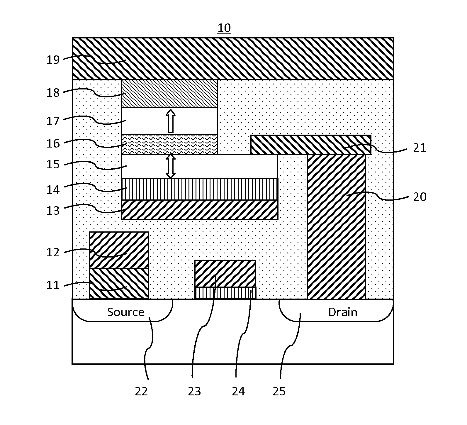
[0052]FIG. 1 is an exemplary cross-section of a magnetoresistive memory cell 10 in a perpendicular STT-MRAM array according to the first embodiment. The magnetoresistive memory cell 10 is configured by a bit line 19, an upper electrode 18, a reference layer 17, a tunnel barrier layer 16, a recording layer 15, an anisotropy modification layer 14, a voltage bias layer 13, and a select transistor comprising an interconnect layer 12, a source contact 11, drain contact 20, a middle electrode 21, source region 22, a gate insulating film 23, a gate electrode 24 and a drain region 25.

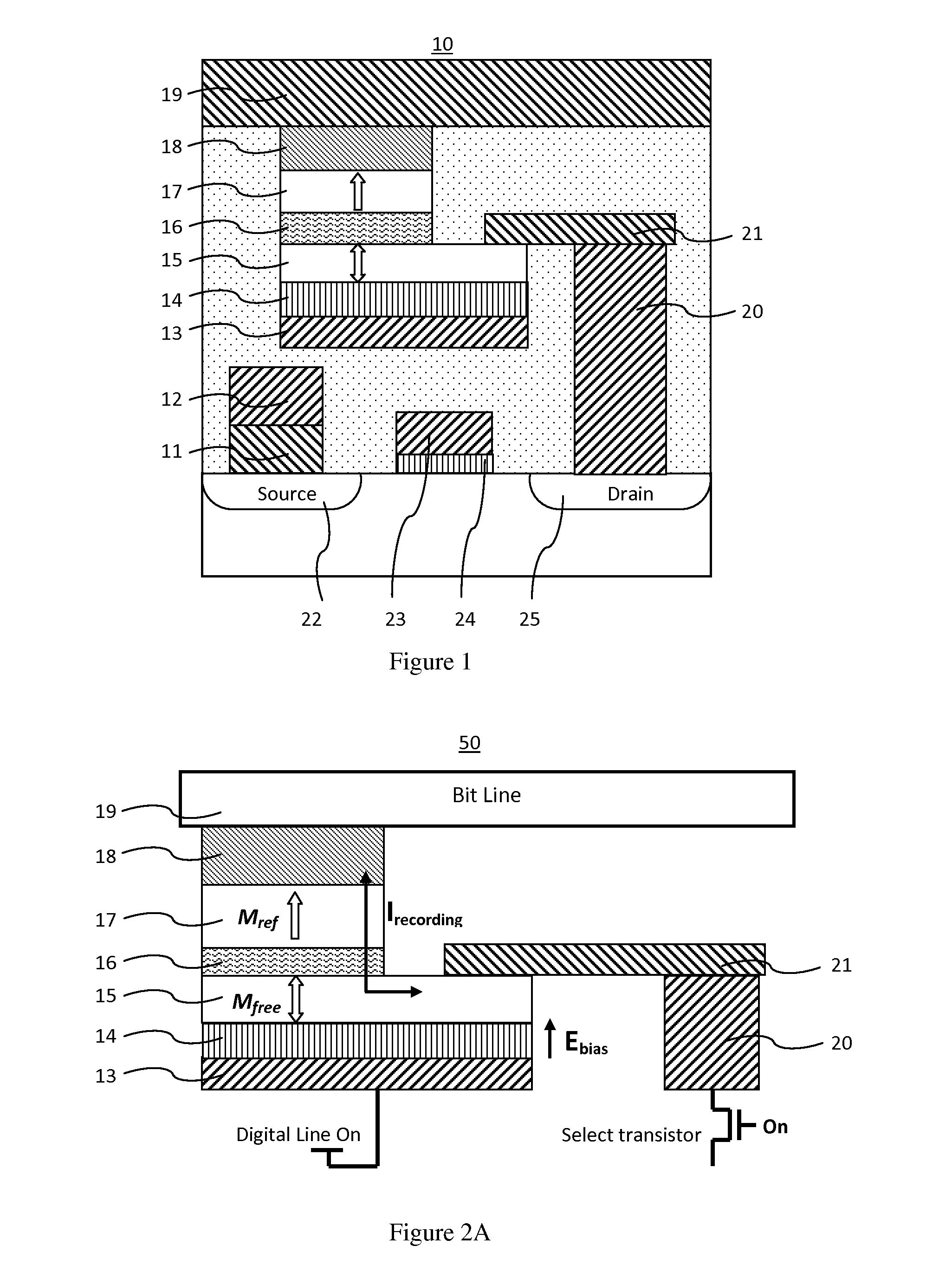
[0053]FIG. 2A illustrates a magnetoresistive element 50 in a recording mode. A circuitry, which is not shown here, is coupled to the bit line for providing a bi-directional recording current between the upper electrode and the middle electrode connecting to the select transistor, and is coupled to the bias layer or digital line for providing a positive voltage on the bias layer in a recording mode. The magnetor...

second embodiment

[0065]FIG. 7 is an exemplary cross-section of a magnetoresistive memory cell 10 in a planar STT-MRAM array according to the second embodiment. The magnetoresistive memory cell 10 is configured by a bit line 19, an upper electrode 18, a reference layer stack 17, a tunnel barrier layer 16, a recording layer 15, an anisotropy modification layer 14, a voltage bias layer 13, and a select transistor comprising an interconnect layer 12, a source contact 11, a middle electrode 21, drain contact 20, a source region 22, a gate insulating film 23, a gate electrode 24 and a drain region 25.

[0066]FIG. 8A illustrates a magnetoresistive element 50 in a recording mode. A circuitry, which is not shown here, is coupled to the bit line for providing a bi-directional recording current between the upper electrode and the middle electrode connecting to the select transistor, and is coupled to the bias layer or digital line for providing a negative voltage on the bias layer in a recording mode. The magnet...


PUM


Abstract

A STT-MRAM comprises apparatus, a method of operating a spin-torque magnetoresistive memory and a plurality of magnetoresistive memory element having a bias voltage controlled perpendicular anisotropy of a recording layer through an interlayer interaction to achieve a lower spin-transfer switching current. The anisotropy modification layer is under an electric field along a perpendicular direction with a proper voltage between a digital line and a bit line from a control circuitry, accordingly, the energy switch barrier is reduced in the spin-transfer recording while maintaining a high thermal stability and a good retention.

Description

RELATED APPLICATIONS[0001]This application claims the priority benefit of U.S. Provisional Application No. 61,751,897, filed on Jan. 13, 2013, which is incorporated herein by reference.BACKGROUND OF THE INVENTION[0002]1. Field of the Invention[0003]This invention relates generally to a spin-transfer-torque magnetic-random-access memory (MRAM) element and a method of manufacturing the same magnetoresistive element, more particularly to structures and methods of reading and programming a spin-torque magnetoresistive random access memory (MRAM) element having a voltage bias controlled writing.[0004]2. Description of the Related Art[0005]In recent years, magnetic random access memories (hereinafter referred to as MRAMs) using the magnetoresistive effect of ferromagnetic tunnel junctions (also called MTJs) have been drawing increasing attention as the next-generation solid-state nonvolatile memories that can cope with high-speed reading and writing, large capacities, and low-power-consum...

Claims


Application Information

Patent Timeline
IPC IPC(8): H01L27/22H01L43/12
CPCH01L43/12H01L27/226G07F17/3204G07F17/3293G11C11/161G11C11/1659G11C11/1673G11C11/1675H10B61/22H10N50/10H10N50/85A63F13/218G06F3/017G11C11/00G11C11/16G11C11/165G11C11/1653G11C11/1655G11C11/1657H01F10/3204H01F10/3209H01L29/82H10B61/00H10B61/20H10N59/00H10N50/00
Inventor GUO, YIMIN
Owner GUO YIMIN
Why Eureka
Try Eureka