Thin-film magnetic device with strong spin polarization perpendicular to the plane of the layers, magnetic tunnel junction and spin valve using such a device

a thin-film magnetic device and perpendicular technology, applied in the field of thin-film magnetic devices with strong spin polarization perpendicular to the plane of the layers, can solve the problems of inadvertent reversal of certain memory cells located on the corresponding row and/or column, write addressing errors, and particular technology is hampered by one serious limitation, so as to improve the adhesion of the layers to each other and the substrate, and enhance the flatness of the layer

Active Publication Date: 2010-10-12
COMMISSARIAT A LENERGIE ATOMIQUE ET AUX ENERGIES ALTERNATIVES +1
View PDF10 Cites 35 Cited by
  • Summary
  • Abstract
  • Description
  • Claims
  • Application Information

AI Technical Summary

Benefits of technology

[0059]Consequently, the thickness of said first layer makes it possible to optimize the spin polarization of an electric current passing through it.
[0062]Generally speaking, the greater the spin polarization, the more the current density required in order to write a memory cell using such a magnetic device or to obtain a radio-frequency oscillator with a wide frequency band can be reduced.
[0065]According to one advantageous aspect, a so-called “buffer layer” made of one or more materials selected from the group comprising tantalum, chromium, titanium, titanium nitride, copper, gold, palladium, silver and / or alloys thereof is interposed between the magnetic device thus defined and the substrate. This buffer layer is more particularly intended to optimize growth of the first and second layers besides improving their adhesion to each other and to the substrate. It also makes it possible to enhance the flatness of said layers because of the adaptation of lattice parameters that it induces. It can also be used to supply current to the base of the device.

Problems solved by technology

This being so, there is a risk of inadvertently reversing certain memory cells located on the corresponding row and / or column having a switching field, possibly located in the lower part of the distribution, that is weaker than the magnetic field generated by the row or column alone.
In other words, this architecture with selection by magnetic fields using rows and columns of conductors can easily result in write addressing errors.
Nevertheless, this particular technology is hampered by one serious limitation.
Because this demagnetizing field is proportional to the magnetization of the material, it is obvious that magnetization reversal makes it necessary to inject a high-intensity current which is capable of damaging the device, especially by causing electric breakdown of the insulating barrier that separates the two magnetic layers in the case of a magnetic tunnel junction.
However, one of the problems encountered with these radio-frequency oscillators is the density of the spin-polarized current that has to be injected into the magnetic system in question and which is capable of causing damage to the device due to breakdown or electromigration phenomena.
However, this may be disadvantageous for some applications in which the wanted signal depends on this magnetization.
If the magnetization that precesses is that of the free (or soft) layer of a tunnel junction deposited on top of the polarising layer, this precession movement results in oscillating variation of the resistance of the stack due to the tunnel magnetoresistance effect of the junction.
In both these cases it seems necessary to grow the magnetic layers by vapour deposition, a technique that is not very compatible with industrial fabrication.
This explains both the need to use such a preparation technique as well as the difficulty in producing such structures.
In addition, these elastic strain effects only occur for certain crystalline magnetic materials.
There is therefore no possibility, for example, of using other magnetic materials or amorphous magnetic alloys.
In addition, no magnetic material other than nickel would give the hoped-for result.
It is evident from the foregoing considerations that none of the proposed solutions can be used to produce, using conventional magnetic materials and a simple preparation method, thin layers with magnetization perpendicular to their plane and having a sufficient “effective” magnetic thickness for the applications in question.

Method used


Image

  • Thin-film magnetic device with strong spin polarization perpendicular to the plane of the layers, magnetic tunnel junction and spin valve using such a device
  • Thin-film magnetic device with strong spin polarization perpendicular to the plane of the layers, magnetic tunnel junction and spin valve using such a device
  • Thin-film magnetic device with strong spin polarization perpendicular to the plane of the layers, magnetic tunnel junction and spin valve using such a device

Examples


first embodiment

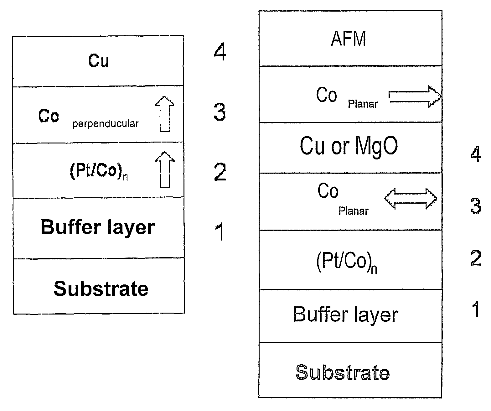
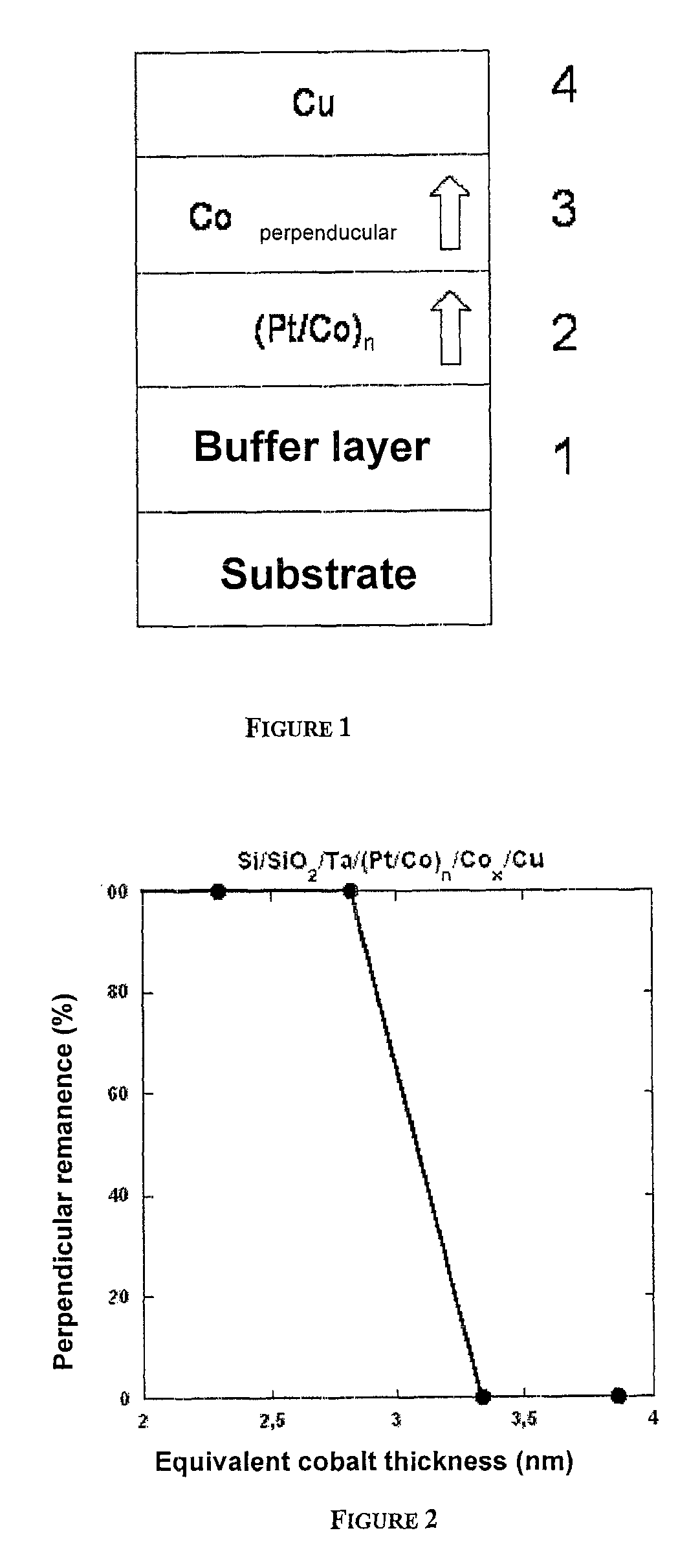
[0093]In the invention, more especially shown in FIG. 1, this buffer layer 1 consists of a thick layer of copper topped by a layer of tantalum and / or platinum. The thickness of the tantalum layer is 2 to 20 nm and advantageously 3 nm. The thickness of the platinum layer is 2 to 30 nm and advantageously 20 nm.

[0094]A layer 2, consisting of a stack of layers of platinum and cobalt in a pattern (Pt / Co)n is then deposited where n is the number of repetitions of the platinum / cobalt stack.

[0095]The thickness of the cobalt layers of multilayer 2 (Co / Pt)n is 0.2 to 1 nm and advantageously 0.6 nm. The thickness of the platinum layers is 0.1 to 2 nm and advantageously roughly 0.3 nm. In addition, the number of repetitions of the stack n (Co / Pt) is 1 to 10.

[0096]A layer 3 made of a ferromagnetic material with a high rate of spin polarization is then deposited on this layer 2. In the example described, this layer 3 is made of cobalt. One can, however, advantageously substitute cobalt by another...

second embodiment

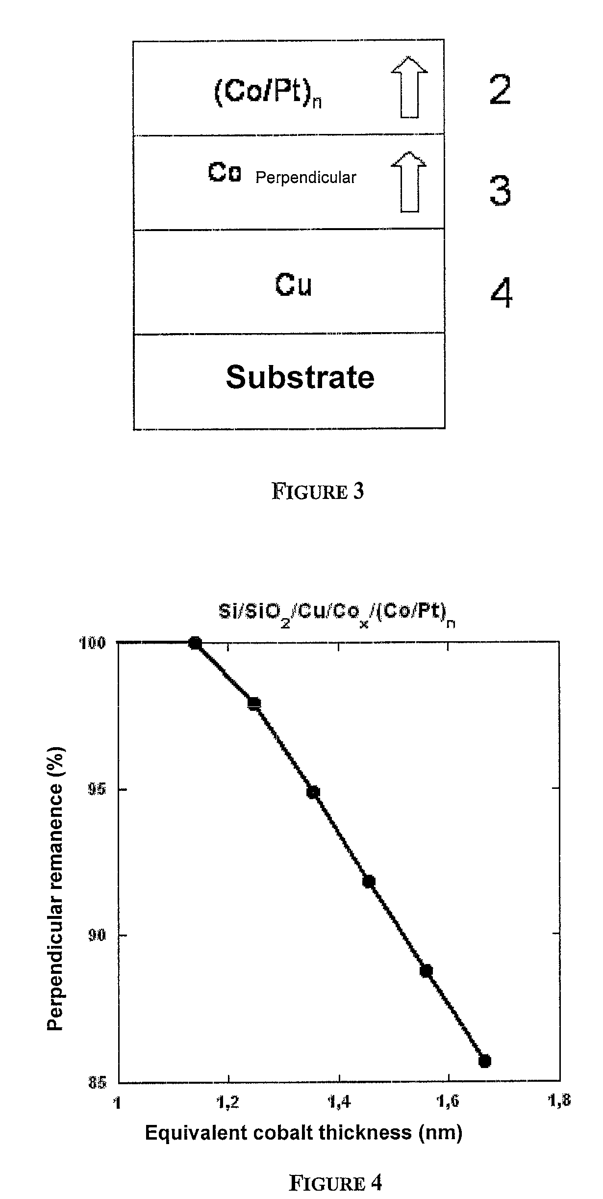
[0122]In a second embodiment, shown in FIG. 3, the structure described in the preceding example is reversed, giving a succession of substrate / copper / cobalt (ferromagnetic material) / multilayer (Co / Pt)n. This embodiment is symmetrical with the preceding embodiment, “effective” cobalt layer 3 now being located, in terms of the sequence in which the various layers are deposited, underneath cobalt / platinum multilayer 2.

[0123]The thickness of the cobalt layers of cobalt / platinum multilayer 2 is 0.2 to 1 nm and advantageously 0.6 nm.

[0124]The thickness of the platinum layers of cobalt / platinum multilayer 2 is 0.2 to 2 nm and advantageously 1.6 nm.

[0125]The number of repetitions of the cobalt / platinum stack is 1 to 10 and advantageously 5.

[0126]FIG. 4 shows, for such a structure, more particularly the Cu / Co / (Co0.6 / Pt1.6)5 / Pt structure, the variation in remanent magnetization, measured with a magnetic field applied perpendicular to the plane of the layers, as a function of the cobalt thickne...

fourth embodiment

[0135]As in the case of the fourth embodiment, this will therefore give a free layer with planar magnetization but a weak demagnetizing field, this free layer being, in this embodiment, located above the anchored layer in terms of the sequence in which the various layers of the device are deposited.


PUM

PropertyMeasurementUnit
thicknessaaaaaaaaaa
thicknessaaaaaaaaaa
magnetic thicknessaaaaaaaaaa

Abstract

A thin-film magnetic device comprises, on a substrate, a composite assembly deposited by cathode sputtering and consists of a first layer made of a ferromagnetic material with a high rate of spin polarization, the magnetization of which is in plane in the absence of any electric or magnetic interaction, a second layer made of a magnetic material with high perpendicular anisotropy, the magnetization of which is outside the plane of said layer in the absence of any electric or magnetic interaction, and coupling of which with said first layer induces a decrease in the effective demagnetizing field of the entire device, a third layer that is in contact with the first layer via its interface opposite to that which is common to the second layer and made of a material that is not magnetic and not polarizing for electrons passing through the device.

Description

CROSS REFERENCE TO RELATED APPLICATIONS[0001]This application claims the benefit under 35 USC §119(e) of U.S. Provisional Application Ser. No. 60 / 868,429, having a filing date of Dec. 4, 2006 and claims the benefit under 35 USC §119(a)-(d) of French Application No. 06.53266, filed Aug. 3, 2006, the entireties of which are incorporated herein by reference.FIELD OF THE INVENTION[0002]The present invention relates to the field of magnetic materials, more especially those intended to be used firstly in non-volatile random-access magnetic memories used to store and read data in electronic systems and secondly in the field of radio-frequency oscillators that use magnetic thin-film systems technology.BACKGROUND OF THE INVENTION[0003]In the field of magnetic memories, so-called M-RAM (Magnetic Random Access Memory) consisting of a magnetic tunnel junction have attracted considerable interest ever since the development of such tunnel junctions which have high magnetoresistance at ambient tem...

Claims


Application Information

Patent Timeline
Patent Type & Authority Patents(United States)
IPC IPC(8): G11B5/39G11C7/00
CPCB82Y25/00G11C11/16H01F10/3236H01F10/3286H01F10/3268H03B15/006G01R33/093G01R33/1284H01F10/3254H01F10/16H01F10/30Y10T428/1121G11C11/161B32B15/04H01F10/08H01F10/32H01F41/18
Inventor RODMACQ, BERNARDDIENY, BERNARD
Owner COMMISSARIAT A LENERGIE ATOMIQUE ET AUX ENERGIES ALTERNATIVES
Why Eureka
Try Eureka