Vanadium Doped SiC Single Crystals and Method Thereof

a technology of silicon carbide and single crystal, which is applied in the direction of crystal growth process, polycrystalline material growth, chemically reactive gas, etc., can solve the problems of unstable and variable vapor pressure of vanadium comprising volatile molecular species, vanadium doping, physical contact between solid vanadium dopant and sic source b,

Active Publication Date: 2014-08-21
II VI DELAWARE INC
View PDF5 Cites 14 Cited by
  • Summary
  • Abstract
  • Description
  • Claims
  • Application Information

AI Technical Summary

Problems solved by technology

A major disadvantage of this type of vanadium doping is the physical contact between the solid vanadium dopant and the SiC source 21.
This makes the partial vapor pressure of the vanadium comprising the volatile molecular species unstable and varying with time, and leads to spatially nonuniform vanadium doping of the grown SiC crystal (such as SiC crystal 24).
The above-cited prior art gas-assisted PVT techniques had potential advantages, such as superior purity and stoichiometry control, but also had limitations and drawbacks.
In the cases of APVT, HTCVD, HCVD and CF-PVT growth, the drawback is the open nature of the growth crucible.
In all of the aforementioned processes, the presence of open passages leads to severe losses of vapors and gases and to very low crystallization efficiency.
These and other drawbacks avoided these techniques from becoming viable commercial competitors to standard PVT sublimation growth.
In the epilayers grown at 1370° C., higher resistivity values were observed, but the epilayer quality was poor.

Method used


Image

  • Vanadium Doped SiC Single Crystals and Method Thereof
  • Vanadium Doped SiC Single Crystals and Method Thereof
  • Vanadium Doped SiC Single Crystals and Method Thereof

Examples


first embodiment

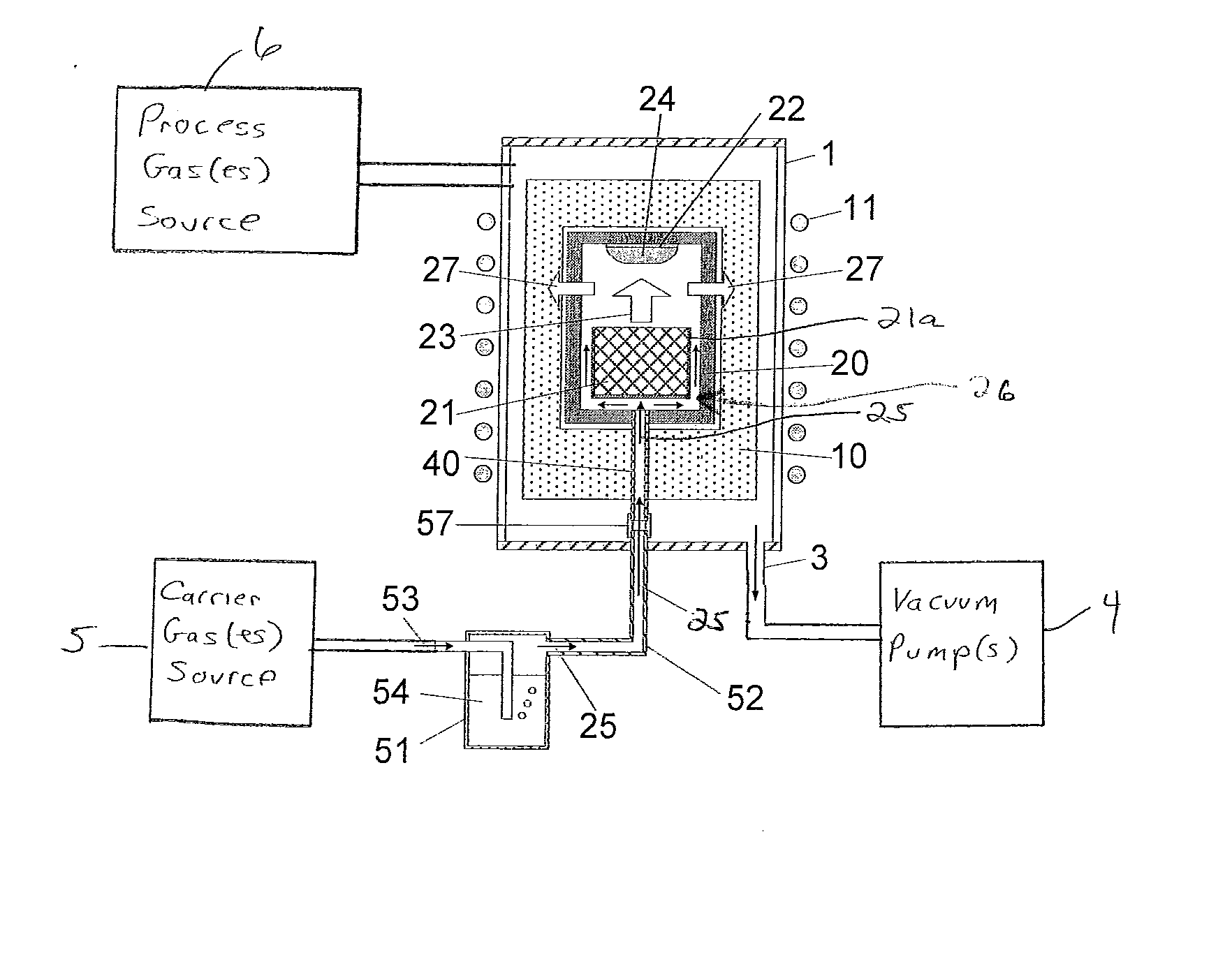
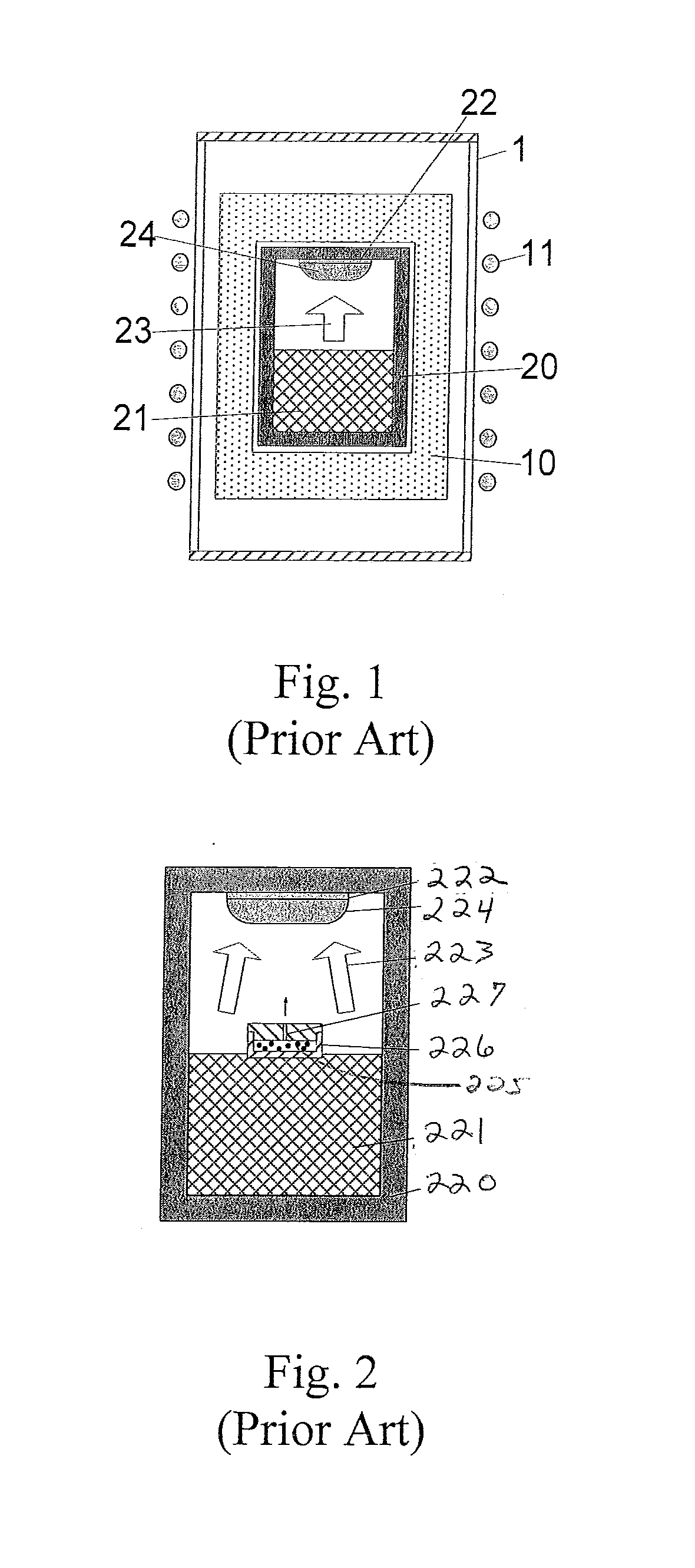
[0064]FIG. 9A shows a SiC crystal growth system in accordance with a first embodiment. In similarity to prior art PVT, growth crucible 20 is placed inside furnace chamber 1, where it is surrounded by thermal insulation 10. Growth crucible 20 is charged with SiC source grain 21 and SiC single crystal seed 22 in spaced relationship: with SiC source grain 21 disposed in the lower portion of growth crucible 20 and SiC single crystal seed 22 disposed in the upper portion of growth crucible 20. Heating of growth crucible 20 is via RF coil 11 (or other suitable heating means). Common and ordinary parts of the SiC crystal growth system of FIG. 10, such as gas and vacuum lines, valves, vacuum pumps, electronic controls, etc. are not shown for simplicity.

[0065]In similarity to the M-PVT process of FIG. 7A, a gas conduit 40 is attached to growth crucible 20. Conduit 40 can be attached at the bottom of the growth crucible 20, as shown in FIG. 9A, or, without limitation, at any other suitable lo...

second embodiment

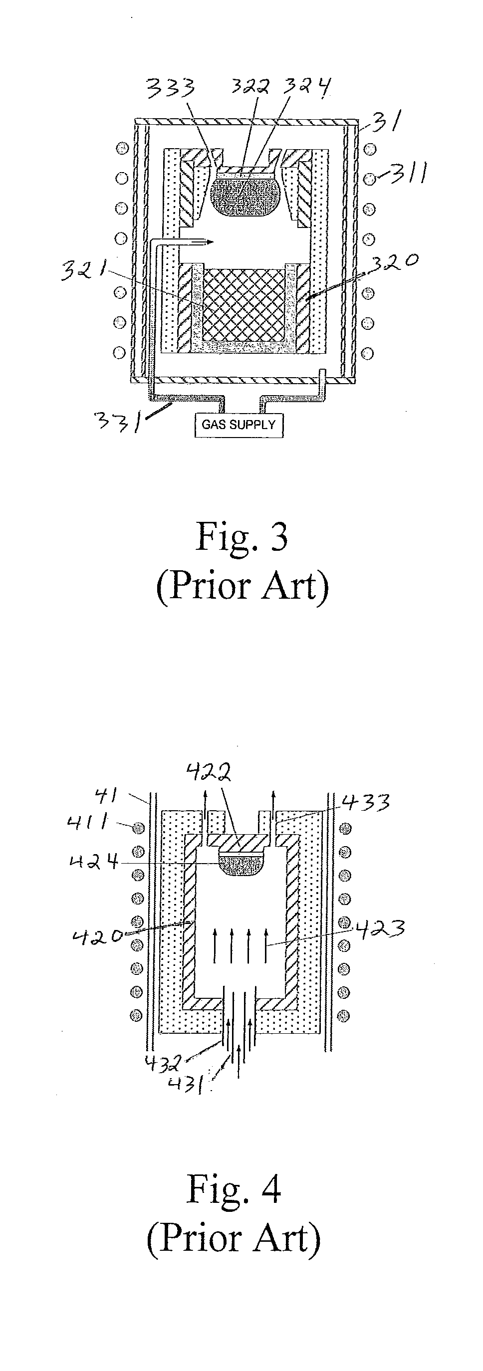
[0083]A second embodiment growth system shown in FIG. 10A is similar in many respects to the first embodiment growth system shown in FIGS. 9A and 9B with the following exceptions: bubbler bath 51 is omitted, carrier gas 53 is introduced directly into gas line 52, and conduit 40 (comprised of upper conduit part 40b and lower conduit part 40a) includes an in-line graphite compartment 41. In similarity to the M-PVT cell shown in FIGS. 7A and 7B, conduit 40 includes graphite compartment 41 situated at a distance from growth crucible 20. Compartment 41 is charged with a solid source of vanadium 42, e.g., in the form of elemental metallic vanadium or solid vanadium compound, such as vanadium carbide (VC).

[0084]Compartment 41 can be disposed in the bulk of thermal insulation 10, as shown in FIG. 10A. In this case, heating of the compartment 41 is provided from the heated growth crucible 20 via thermal conductivity along conduit 40. Also or alternatively, thermal insulation 10 can be carved...


PUM

PropertyMeasurementUnit
temperatureaaaaaaaaaa

Abstract

A sublimation grown SiC single crystal includes vanadium dopant incorporated into the SiC single crystal structure via introduction of a gaseous vanadium compound into a growth environment of the SiC single crystal during growth of the SiC single crystal.

Description

CROSS REFERENCE TO RELATED APPLICATION[0001]The present invention claims priority from U.S. Provisional Patent Application No. 61 / 767,318, filed Feb. 21, 2013, the disclosure of which is hereby incorporated in its entirety by reference.BACKGROUND OF THE INVENTION[0002]1. Field of the Invention[0003]The present invention relates to silicon carbide (SiC) single crystals and, more particularly, to a method of fabricating SiC single crystals using a gaseous source of deep level dopant.[0004]2. Description of Related Art[0005]Single crystals of silicon carbide of 4H and 6H polytypes serve as lattice-matched substrates in SiC- and AlGaN-based semiconductor devices, including ultra-high-frequency AlGaN-based transistors and SiC-based devices for power switching. Other applications include ultra-fast photoconductive switches, sensors for harsh environments, radiation detectors and many others. In the cases of high-frequency devices and photoconductive switches, the SiC substrates must be se...

Claims


Application Information

Patent Timeline
Patent Type & Authority Applications(United States)
IPC IPC(8): C30B23/02C30B29/36
CPCC30B29/36C30B23/02C30B23/00
Inventor ZWIEBACK, ILYAANDERSON, THOMAS E.GUPTA, AVINASH K.NOLAN, MICHAEL C.BROUHARD, BRYAN K.RULAND, GARY E.
Owner II VI DELAWARE INC
Why Eureka
Try Eureka