Layered composite of a substrate film and of a layer assembly comprising a sinterable layer made of at least one metal powder and a solder layer

a technology of layered composite and substrate film, which is applied in the direction of soldering apparatus, superimposed coating process, manufacturing tools, etc., can solve the problems of lead-containing solder joining, assembly failure, and thermal stress of electric or electronic components present, and achieve the effect of reducing the number of legal restrictions

Inactive Publication Date: 2014-08-21
ROBERT BOSCH GMBH
View PDF9 Cites 12 Cited by
  • Summary
  • Abstract
  • Description
  • Claims
  • Application Information

AI Technical Summary

Benefits of technology

[0011]The term sinterable layer can refer, in particular, to a layer of a sinterable or at least partially presintered material containing at least one metal powder. In particular, the sinterable layer can be configured as preshaped, for example sheet-like shaped body (sinter sheet). Such a preshaped shaped body can also be referred to as preform or sinter molding. The material of the sinterable layer can have been dried, partially sintered and / or fully sintered to form the preform. Such a sinter molding has the advantage that it can have an open porosity. Previously integrated stable gas channels of the sinter molding can then allow ventilation and deaeration of a join produced, for example, by soldering. A particularly stable join to a join partner can be produced in this way and crack formation during joining can be largely avoided, especially when large-area join partners, for example silicon power semiconductors and circuit substrates or heat sinks are used and are joined to one another. The sinter layer, in particular sinter moldings, can also expand the freedom of choice in the design of a join since, for example, the sinter molding can have a larger area than at least one of the join partners and / or the join partners can be spaced substantially further apart than in the case of direct sintering of the join partners by means of a metal paste. The temperature-change resistance of the resulting electronic components can be increased in this way.
[0054]To produce a join between, for example, an electronic power component and a substrate, the power component is firstly placed on the solder layer of the layer composite formed according to the invention with support film. To establish adhesion between the layer composite composed of solder layer and sinterable layer and the power component, the loose assembly is subjected to pressure, for example in the range from 20 MPa to 80 MPa, and / or elevated temperature, for example in the range from 40° C. to 80° C. Overall, adhesion of this type which is greater than the adhesion between the support film and the composite is desired between the layer composite and the component, so that the support film can be removed without delamination of the component. After lifting off from the support film, for example by means of a take-off device as is known as “pick-and-place robot” in mass production, the composite of layer arrangement and component can now be placed on the join partner, for example a substrate. The substrate can thus optionally likewise be provided with a sinterable layer or with a solder layer on the surface to be joined. In a subsequent process step, adhesion is established between the substrate and the composite with the component by application of pressure and / or heat. Here, intermetallic phases can be formed between the component surface, the solder layer, the sinterable layer and the substrate surface and these can make a high temperature-resistant and mechanically stable electrical connection having excellent conductivity and equalization properties in respect of the greatly differing coefficients of thermal expansion of the two elements to be joined possible.

Problems solved by technology

The currents necessary in power electronics lead to thermal stressing of the electric or electronic components present.
Further thermal stressing results from the use of such electric or electronic appliances at operating locations in which the temperature is substantially above room temperature and may even change continually.
However, particularly at use temperatures close to the melting point, such joining layers display deteriorating electrical and mechanical properties which can lead to failure of the assembly.
However, lead-containing solder joins are subject to a number of legal restrictions in terms of their permissible industrial uses for reasons of environmental protection.
Lead-free hard solders generally have a melting point above 200° C. However, when hard solder is used to form a joining layer, there are only a few electrical or electronic components which are possible as join partners which can withstand the high temperatures during melting of the hard solders.
However, when temperature changes occur, thermomechanical stresses and even crack formation in semiconductor components or even in the support substrate can occur in the case of such sintered joins.
Particularly in the case of electronic components, higher power losses and progressive miniaturization also lead to an overall increase in the use temperatures.

Method used


Image

  • Layered composite of a substrate film and of a layer assembly comprising a sinterable layer made of at least one metal powder and a solder layer

Examples


Embodiment Construction

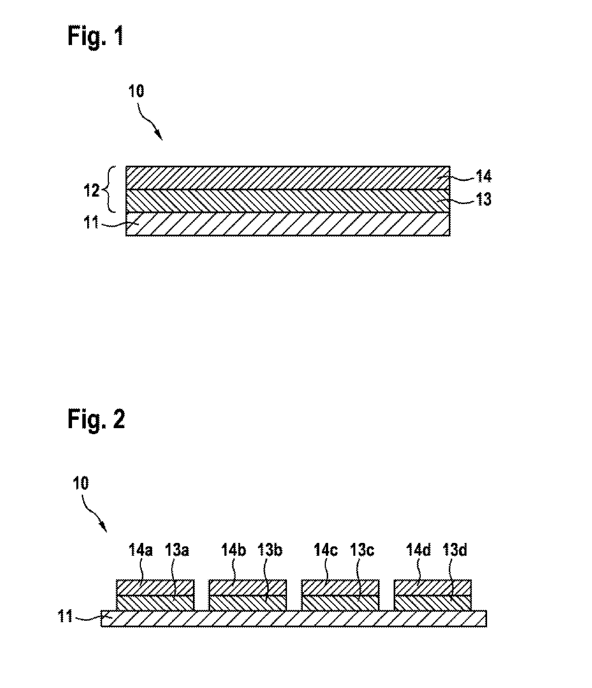
[0060]FIG. 1 shows a layer composite 10 comprising at least one support film 11 and a layer arrangement 12 applied thereto. The support film can be a polymer film, in particular a polyester film. According to the invention, the layer arrangement 12 comprises at least one sinterable layer 13 which contains at least one metal powder and has been applied to the support film 11, and a solder layer 14 applied to the sinterable layer. The sinterable layer 13 is composed of silver or a silver alloy, copper or a copper alloy and optionally a solvent. An additive which can, in particular, serve as redox partner can optionally be used in addition. The material of the solder layer 14 is selected from the group consisting of SnCu, SnAg, SnAu, SnBi, SnNi, SnZn, SnIn, SnIn, CuNi, CuAg, AgBi, ZnAl, BiIn, InAg, InGa and ternary or quaternary alloys of a mixture thereof and is preferably lead-free. The layer composite 10 can be used, in particular, for joining electronic components as join partners....


PUM

PropertyMeasurementUnit
thicknessaaaaaaaaaa
thicknessaaaaaaaaaa
temperatureaaaaaaaaaa

Abstract

The invention relates to a layered composite (10), in particular for connecting electronic components as joining partners, comprising at least one substrate film (11) and a layer assembly (12) applied to the substrate film. The layer assembly comprises at least one sinterable layer (13), which is applied to the substrate film (11) and which contains at least one metal powder, and a solder layer (14) applied to the sinterable layer (13). The invention further relates to a method for forming a layered composite, to a circuit assembly containing a layered composite (10) according to the invention, and to the use of a layered composite (10) in a joining method for electronic components.

Description

BACKGROUND OF THE INVENTION[0001]The invention relates to a layer composite, in particular for joining electronic components as join partners, a process for forming such a layer composite and also a circuit arrangement and the use in a joining process.[0002]Power electronics are used in many fields of technology. In electric or electronic appliances in which high currents flow, the use of power electronics is particularly indispensible. The currents necessary in power electronics lead to thermal stressing of the electric or electronic components present. Further thermal stressing results from the use of such electric or electronic appliances at operating locations in which the temperature is substantially above room temperature and may even change continually. Examples of this which may be mentioned are control systems in the automobile sector which are arranged directly in the engine compartment.[0003]A particularly large number of connections between power semiconductors or integr...

Claims


Application Information

Patent Timeline
Patent Type & Authority Applications(United States)
IPC IPC(8): B23K35/02B32B15/06B23K1/00B32B15/16
CPCB23K35/0238B32B15/16B23K2001/12B23K1/0016B32B2264/105B32B15/06C23C26/00H01L24/29H01L24/83H01L2224/8384H01L2924/10253H01L2924/14H01L2224/27003H01L2224/27848H01L2224/271H01L2224/29239H01L2224/29247H01L2224/27334H01L24/27H01L2224/27505H01L2224/278H01L2224/29082H01L2224/29109H01L2224/29111H01L2224/29139H01L2224/29147H01L2224/29211H01L2224/293H01L2224/29339H01L2224/29347H01L2224/29355H01L2224/32503H01L2224/83191H01L2224/83193H01L2224/832H01L2224/83203H01L2224/83815H01L2924/01327H01L2224/29118H01L2224/29113H01L2224/29395H01L2224/29218H01L2224/29213H01L2224/29209H05K3/3478H05K2203/1131H05K2203/0405H01L2924/351C23C28/021C23C28/023H01L2224/8382H01L2924/07811B23K1/0008H01L2924/15787H01L2924/12042Y10T428/12063Y10T428/12049H01L2924/00013H01L2924/01029H01L2924/01047H01L2924/01079H01L2924/01083H01L2924/01028H01L2924/0103H01L2924/01049H01L2924/01013H01L2924/01031H01L2924/0132H01L2924/00
Inventor KALICH, THOMASWETZL, FRANKHOHENBERGER, BERNDHOLZ, RAINERFRUEH, CHRISTIANEFIX, ANDREASGUYENOT, MICHAELFEIOCK, ANDREARITTNER, MARTINGUENTHER, MICHAEL
Owner ROBERT BOSCH GMBH
Why Eureka
Try Eureka