Gamma detector based on geigermode avalanche photodiodes

Inactive Publication Date: 2014-09-04
UNIV TUBINGEN
View PDF7 Cites 15 Cited by
  • Summary
  • Abstract
  • Description
  • Claims
  • Application Information

AI Technical Summary

Benefits of technology

The invention provides a detector with a reduced number of readout circuits, which reduces the electronic effort needed to obtain the same information as using a one-to-one coupling of individual scintillation crystals with a single G-APD sensor element. Only one or two readout circuits are needed for a row of several G-APD sensor elements, which doubles the number of G-APD sensor elements and allows for quick and easy determination of the location of the light in the x / y plane of the first and second surface. The arrangement also allows for information on the Depth Of Interaction (DOI) which provides information where the gamma ray was absorbed within the height of the scintillation crystal block. The use of single crystals arranged in a matrix block provides more precise detection of the location of the light generated by the gamma rays.

Problems solved by technology

These light detectors are bulky and relatively cost-intensive and are not suited for multimodality medical imaging devices.
However, the big disadvantage of a one-to-one coupling is the required large number of readout channels.
A major problem which strikes researchers and engineers when designing a high resolution PET scanner is that they have to make a compromise between spatial resolution and sensitivity.
The parallax error is especially predominant in small bore scanners like animal scanners.
However, having short crystals is highly counterproductive to the sensitivity since the stopping probability for commonly used gamma quanta is increased by the crystal length.
Thus, the prior art discussed in so far still does not teach how to design a Gamma Detector that has simple overall construction, uses an as small as possible number of electronic readout channels and provides high spatial resolution and high sensitivity.

Method used


Image

  • Gamma detector based on geigermode avalanche photodiodes
  • Gamma detector based on geigermode avalanche photodiodes
  • Gamma detector based on geigermode avalanche photodiodes

Examples


Embodiment Construction

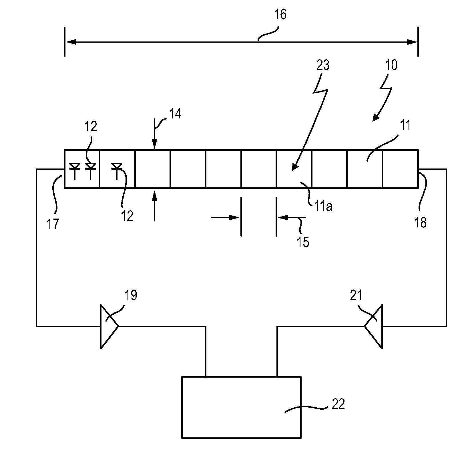
[0045]In FIG. 110 denotes an elongate strip of ten G-APD sensor elements 11, wherein each sensor element 11 comprises 1.000 or even more single diodes or cells 12. As an example, some cells 12 are shown in FIG. 1.

[0046]The G-APD sensor elements 11 are arranged one beside another in a row to form an elongate G-APD strip 10. Each G-APD sensor element 11 has a width indicated at 14 and a length indicated at 15. The overall length of the G-APD strip 10 as indicated at 16 thus corresponds to ten times length 15.

[0047]The G-APD sensor elements 11 form an integral strip 10 that is logically divided into ten single G-APD sensor elements 11 each of length 15. It may also be the case that ten discrete G-APD sensor elements 11 are arranged in a row to form the strip 10, whereby adjacent G-APD sensor elements 11 then are electrically connected to each other. The strip 10 may also be monolithic having a length 16 and ten times the number of cells 12 than one discrete G-APD sensor element 11.

[004...


PUM


Abstract

A Gamma Detector (25) comprises a scintillation crystal block (26) and a set of Geigermode Avalanche Photodiode (G-APD) sensor elements (11) optically coupled to at least a first surface (27) of the scintillation crystal block (26). The G-APD sensor elements (11) are arranged in at least one elongate strip (10) of G-APD sensor elements (11), said G-APD strip (10) coupled to a readout circuit at one, preferably at both of its ends (FIG. 2).

Description

BACKGROUND OF THE INVENTION[0001]The present invention relates to a Gamma Detector comprising a scintillation crystal block and a set of Geigermode Avalanche Photodiode (G-APD) sensor elements optically coupled to at least a first surface of the scintillation crystal block.[0002]Such Gamma Detectors are used for medical, military and security purposes. They comprise one or more scintillation crystals to convert gamma radiation into light. They further comprise one or more highly sensitive light detectors. One application for Gamma Detectors is in the field of Positron Emission Tomography (PET).[0003]PET is a nuclear medicine imaging technique that produces a three-dimensional image of functional processes in a human or animal body. The detection is based on positrons emitted by a radionuclide, a so called tracer, which tracer is introduced into the body together with a biologically active or tolerable molecule. During decay, the tracer emits a positron which travels for a short dist...

Claims


Application Information

Patent Timeline
IPC IPC(8): G01T1/202G01T1/20
CPCG01T1/2018G01T1/202G01T1/1644G01T1/248G01T1/208G01T1/20183G01T1/20186G01T1/20185
Inventor PICHLER, BERNDKOLB, ARMINLORENZ, ECKART
Owner UNIV TUBINGEN
Why Eureka
Try Eureka