
Memory device

a memory device and memory technology, applied in the field of memory devices, can solve the problems of high demand for buffer memory devices, leakage power reduction, and increased power consumption of semiconductor elements, and achieve the effects of low power consumption, reduced number of elements, and small circuit siz

Active Publication Date: 2014-09-18
SEMICON ENERGY LAB CO LTD
View PDF8 Cites 4 Cited by
  • Summary
  • Abstract
  • Description
  • Claims
  • Application Information

AI Technical Summary

Benefits of technology

The present invention provides a memory device with a novel structure that has several technical effects. Firstly, it reduces the number of elements needed, making it more efficient. Secondly, it reduces the layout area needed, making it more compact. Lastly, it reduces power consumption, making it more energy-efficient. Overall, this invention allows for a smaller and more efficient memory device with low power consumption.

Problems solved by technology

However, the miniaturization of the semiconductor elements increases power consumption (leakage power) due to leakage current of the transistors in the CPUs.
Specifically, most of power consumption of conventional CPUs is power consumption (operation power) at the time of calculations, while leakage power accounts for at least 10% of power consumption of CPUs in recent years.
In particular, in a CPU for portable devices such as mobile phones and portable information terminals, registers and buffer memory devices such as caches occupy more than or equal to half a chip area of the CPU or use more than or equal to half the number of transistors; therefore, a reduction in leakage power of the buffer memory devices is highly demanding.
As such a nonvolatile memory, a magnetic element or a ferroelectric element can be used; however, the use of such elements makes the manufacturing process of a semiconductor device complicated.
A latch portion in Patent Document 1 includes a large number of elements and therefore has a problem of an increase in a layout area.

Method used


Image

  • Memory device
  • Memory device
  • Memory device

Examples


embodiment 1

[0050]In this embodiment, a structure of a memory device of one embodiment of the disclosed invention is described. Note that in a block diagram attached to this specification, components are classified according to their functions and shown as independent blocks; however, it is practically difficult to completely separate the components according to their functions, and one component may have a plurality of functions.

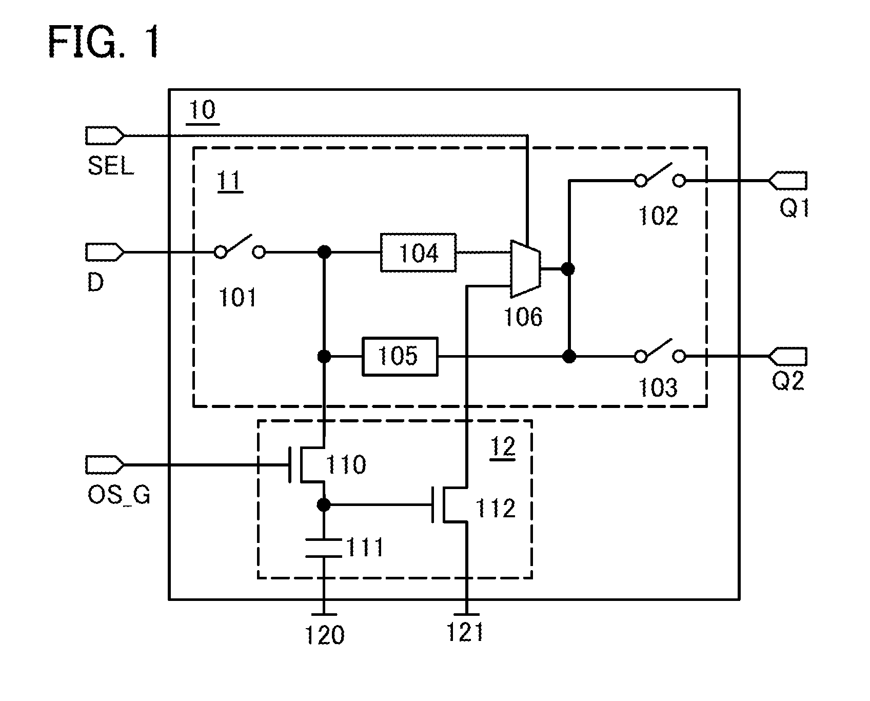
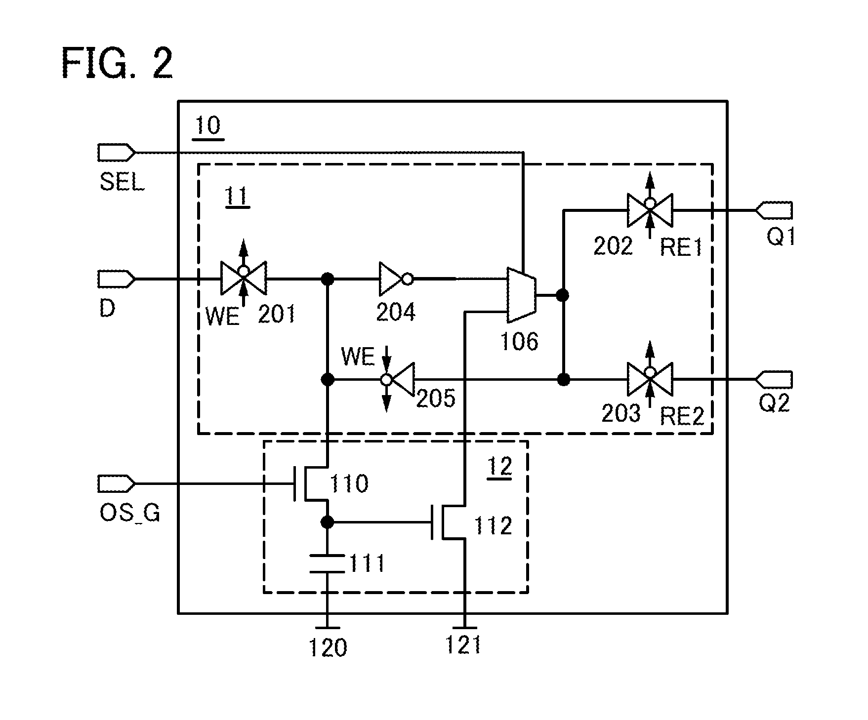
[0051]FIG. 1 illustrates one example of a structure of a memory device. A memory device 10 includes a memory circuit 11 and a memory circuit 12. A first terminal of the memory circuit 11 is connected to a first terminal of the memory circuit 12, and a second terminal of the memory circuit 11 is connected to a second terminal of the memory circuit 12.

[0052]The memory circuit 11 includes a logic element 104, a logic element 105, a selection circuit 106, a switch 101, a switch 102, and a switch 103. The logic element 105 and the logic element 104 can also be referred to a...

embodiment 2

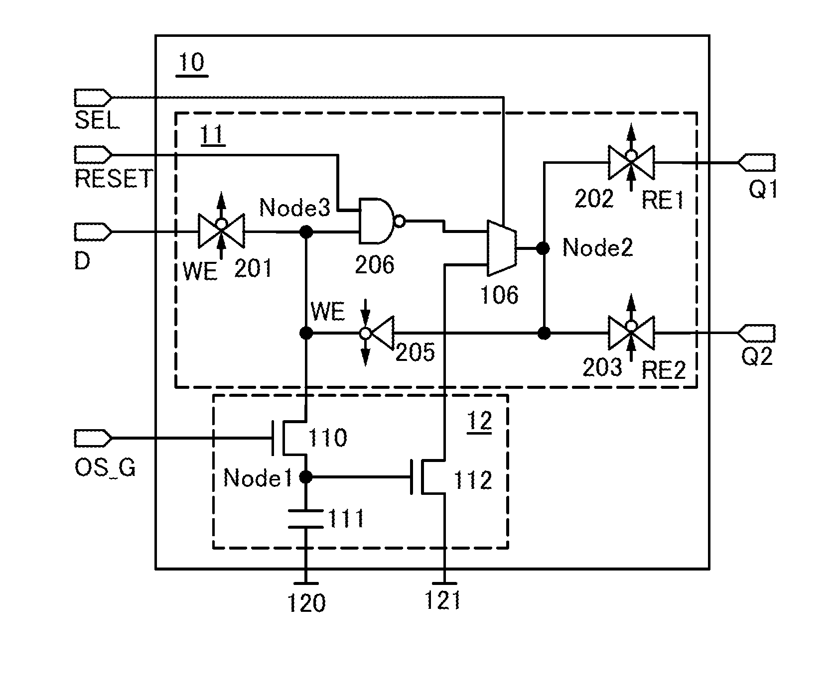
[0120]FIG. 9 illustrates an example of a memory device with a structure different from those in Embodiment 1.

[0121]The memory device 10 includes the memory circuit 11, the memory circuit 12, and a memory circuit 13.

[0122]The memory circuit 11 includes the transmission gates 201 to 203, the clocked inverter 205, the NAND 206, and the selection circuit 106.

[0123]The memory circuit 12 includes the n-channel transistor 110, the n-channel transistor 112, an n-channel transistor 901, and the capacitor 111. It is preferable that the off-state current of the transistor 110 be extremely small. For example, a channel region of the transistor 110 is preferably formed using an oxide semiconductor. In addition, a channel region of the transistor 112 is preferably formed using silicon, for example. Note that the channel region of the transistor 112 can be formed using an oxide semiconductor.

[0124]The memory circuit 13 includes an n-channel transistor 902, an n-channel transistor 903, a p-channel ...

embodiment 3

[0146]In this embodiment, description is given of a specific embodiment of a CPU corresponding to one mode of a semiconductor device of the present invention.

[0147]FIG. 10 is a block diagram illustrating an example of a structure of a CPU. Although the block diagram attached to this specification illustrates components classified by their functions in independent blocks, it is difficult to classify actual components according to their functions completely and it is possible for one component to have a plurality of functions.

[0148]A CPU 600 includes a control unit 601, an arithmetic logic unit (ALU) 602 corresponding to an arithmetic unit, a data cache 603, an instruction cache 604, a program counter 605, an instruction register 606, a main memory device 607, and a register file 608.

[0149]The control unit 601 is configured to decode and carry out an instruction which is input. The ALU 602 is configured to perform a variety of arithmetic operations such as four arithmetic operations a...


PUM


Abstract

A memory device with a novel structure that is suitable for a register file is provided. The memory device includes a first memory circuit and a second memory circuit. The first memory circuit includes a first logic element and a second logic element each of which is configured to perform logic inversion, a selection circuit, a first switch, a second switch, and a third switch. The second memory circuit includes a first transistor in which a channel formation region is provided in an oxide semiconductor film, a second transistor, and a capacitor to which a potential is supplied through the first transistor.

Description

BACKGROUND OF THE INVENTION[0001]1. Field of the Invention[0002]The present invention relates to an object, a method, or a manufacturing method. In addition, the present invention relates to a process, a machine, or manufacture. In particular, the present invention relates to, for example, a semiconductor device, a memory device, a display device, a light-emitting device, a power storage device, an electronic device, a driving method thereof, or a manufacturing method thereof. In particular, the present invention relates to a memory device and a semiconductor device using the memory device.[0003]2. Description of the Related Art[0004]In semiconductor devices such as central processing units (CPUs), semiconductor elements have been miniaturized and circuits have been made smaller in size to increase integration degree, and now transistors with a channel length of approximately 30 nm are manufactured. However, the miniaturization of the semiconductor elements increases power consumpti...

Claims


Application Information

Patent Timeline
IPC IPC(8): G11C11/24G11C5/14
CPCG11C5/14G11C11/24G11C11/403G11C2207/007H01L27/1225H10B41/70G11C14/0054
Inventor OHMARU, TAKURO
Owner SEMICON ENERGY LAB CO LTD
Learn More