Dicing Sheet with Protective Film Forming Layer and Chip Fabrication Method

a technology of dicing sheet and protective film, which is applied in the direction of film/foil adhesives, layered products, transportation and packaging, etc., can solve the problems of product yield rate decline, and achieve the effect of easy formation and excellent printing accuracy

Active Publication Date: 2014-10-02
LINTEC CORP
View PDF12 Cites 76 Cited by
  • Summary
  • Abstract
  • Description
  • Claims
  • Application Information

AI Technical Summary

Benefits of technology

[0033]When forming the protective film to the backside of the semiconductor chip, by using the dicing sheet with the protective film forming layer according to the present invention, the thickness of the backside of the semiconduct

Problems solved by technology

However, the accuracy of the thickness of the protective film formed as such

Method used


Image

  • Dicing Sheet with Protective Film Forming Layer and Chip Fabrication Method
  • Dicing Sheet with Protective Film Forming Layer and Chip Fabrication Method
  • Dicing Sheet with Protective Film Forming Layer and Chip Fabrication Method

Examples


example 1

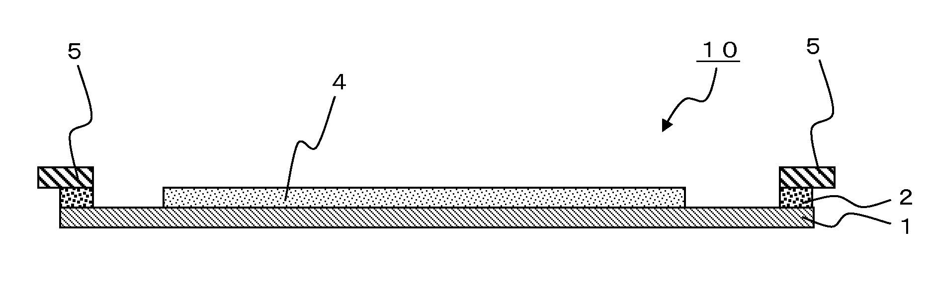
[0203]The above mentioned each components of the protective film forming layer composition were blended by the above mentioned blended amount. Also, as the release sheet, polyethylenetelephthalate film (SP-PET 381031, thickness of 38 μm, the surface tension of less than 30 mN / m, the melting point of 200° C. or higher, made by Lintec Corporation) carried out with the release treatment at the one side were prepared.

[0204]Methylethylketone solution of the above mentioned protective film forming layer composition (the solid concentration of 61 wt %) was coated on the release treatment face of the above mentioned release sheet so that the thickness after drying is 25 μm, and dried (the drying condition: 120° C. for 3 minutes in the oven); thereby the protective film forming layer was formed on the release sheet. Next, the protective film forming layer on the release sheet was cutout as the same size as (the diameter of 8 inch) the silicon wafer, and the protective film forming layer whic...

example 2

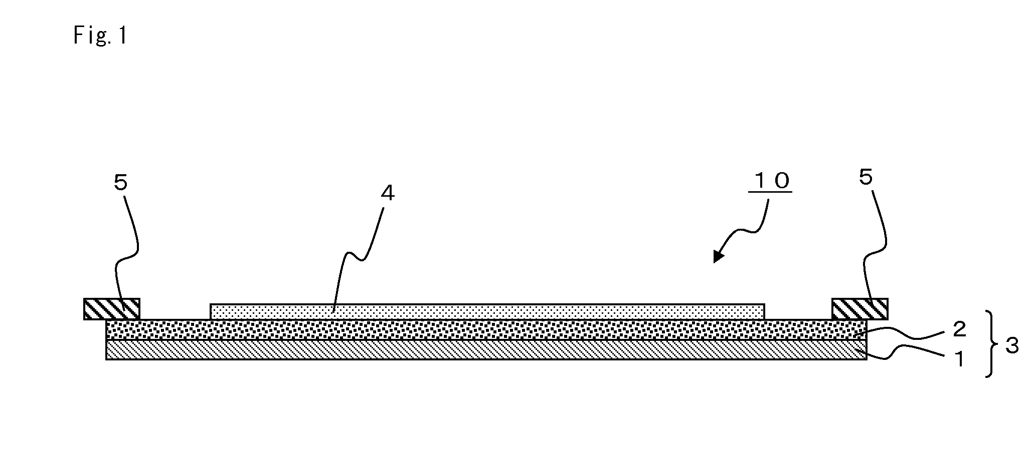
[0207]The dicing sheet with the protective film forming layer was obtained as same as the example 1 except that polypropylene film having the thickness of 50 μm (suntox-CP KT made by SunTox Co., Ltd.) carried out with the corona treatment was used as the base film. Each evaluation results are shown in Table 1.

example 3

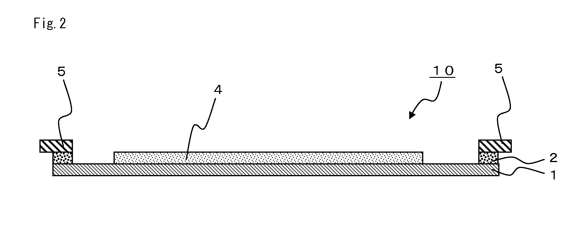
[0208]The dicing sheet with the protective film forming layer was obtained as same as the example 1 except for using polybutylenetelephthalate film having the thickness of 100 μm as the base film. Each evaluation results are shown in Table 1.


PUM


Abstract

A dicing sheet with a protective film forming layer has a substrate film, an adhesive layer, and a protective film forming layer, and at a minimum, the adhesive layer is formed in an area surrounding the protective film forming layer in a planar view, and the substrate film has the following characteristics (a)-(c): (a) the melting point either exceeds 130° C. or the film has no melting point; (b) the thermal contraction rate under conditions of heating at 130° C. for two hours is from −5 to +5%, and (c) the degree of elongation-to-break in the MD direction and the CD direction is at least 100%, and the stress at 25% is no more than 100 MPa.

Description

TECHNICAL FIELD[0001]The present invention relates to a dicing sheet with a protective film forming layer capable of forming a protective film at the backside of the chip and also capable of improving the production efficiency of the chip. Also, the present invention relates to a production method of the chip using the dicing sheet with the protective film forming layer.DESCRIPTION OF THE RELATED ART[0002]Recently, the production of the semiconductor device using the mounting method of so called “face down method” is carried out. In the face down method, the semiconductor chip (hereinafter, it may be referred as “chip”) having electrodes such as bumps or so on the circuit surface is used, and said electrodes are bonded with the substrate. Therefore, the face of the opposite side of the circuit face of the chip (the backside of the chip) will be exposed.[0003]The chip backside which has been exposed may be protected by an organic film. Conventionally, the chip having the protective f...

Claims


Application Information

Patent Timeline
IPC IPC(8): H01L21/78H01L21/683H01L21/304C09J7/40
CPCH01L21/78C09J2201/622H01L21/6836H01L21/304C09J201/00H01L2221/68327C09J7/0225C09J2203/326H01L23/544H01L2221/68377H01L2223/54406H01L2223/54433H01L2223/54486H01L2924/0002Y10T428/24843C09J7/40C09J2301/312H01L2924/00H01L21/30
Inventor SHINODA, TOMONORIFURUDATE, MASAAKITAKANO, KEN
Owner LINTEC CORP
Why Eureka
Try Eureka