HEMT transistors consisting of (iii-b)-n wide bandgap semiconductors comprising boron

a technology of boron and hemt, which is applied in the direction of semiconductor devices, semiconductor/solid-state device details, electrical apparatus, etc., can solve the problems of inability to obtain a naturally resistive iii-v material, heterostructures that have in practice proved disappointing, and difficulty in practical industrial implementation of this solution. achieve the effect of preventing electron leakage, increasing the resistivity of the structure, and promoting electron confinemen

Inactive Publication Date: 2014-11-06
THALES SA +4
View PDF8 Cites 21 Cited by
  • Summary
  • Abstract
  • Description
  • Claims
  • Application Information

AI Technical Summary

Benefits of technology

[0022]Regarding the invention, the inventors thus had the idea of using a semi-insulating BGaN layer as an electrostatic barrier, rather than InGaN under the channel. Advantage is then taken of a double effect, a potential barrier effect promoting confinement of electrons in the potential well, due to the strong electronic polarization of the BGaN layer, and an increase in the resistivity of the structure under the channel, preventing leakage of electrons into the substrate, due to the resistive nature of this layer.
[0023]These two effects are obtained for small amounts of boron, 0.1% or more, allowing such a structure to be easily produced with prior-art techniques.

Problems solved by technology

However, it is difficult to obtain a III-V material that is naturally resistive.
These heterostructures have in practice proved to be disappointing, when employed at microwave frequencies, due to a significant increase in the amount of impurities in the structure irreversibly creating traps that are sources of degradation in the performance of the transistor.
However, practical industrial implementation of this solution proves to be difficult on account of the very different temperatures used to grow the various materials of this structure.
However, it is not possible to envision lowering the growth temperature of GaN, because this would lead to a reduction in its structural and electronic qualities.
It is also not possible to envision passing, in a few fractions of a second, at the InGaN / GaN interface, from 700° C. to 1000° C.: this would have very disadvantageous effects on the electronic properties of the GaN material and on the structural properties of the InGaN material, there notably being a risk of breakage.

Method used


Image

  • HEMT transistors consisting of (iii-b)-n wide bandgap semiconductors comprising boron
  • HEMT transistors consisting of (iii-b)-n wide bandgap semiconductors comprising boron
  • HEMT transistors consisting of (iii-b)-n wide bandgap semiconductors comprising boron

Examples


Embodiment Construction

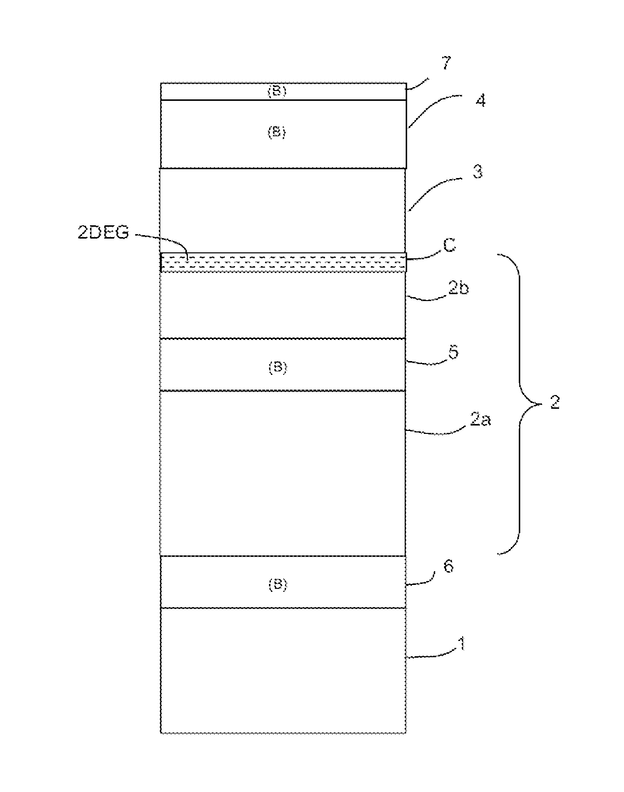
[0047]By way of introduction it will be noted that the figures illustrating the stacks of layers of the electronic structure are not drawn to scale. Notably, the thicknesses shown are not proportional. Moreover, for the sake of simplicity with respect to references, elements common to all the structures have been given the same references.

[0048]The invention will in particular be described with regard to a nonlimiting example application to an electronic structure for a HEMT transistor based on the III-nitrides, and more particularly on an AlGaN / GaN heterojunction. AlGaN is the material M2 of the barrier layer having a bandgap Egg that is wider than that Eg1 of the first material M1 of the buffer layer, which is GaN.

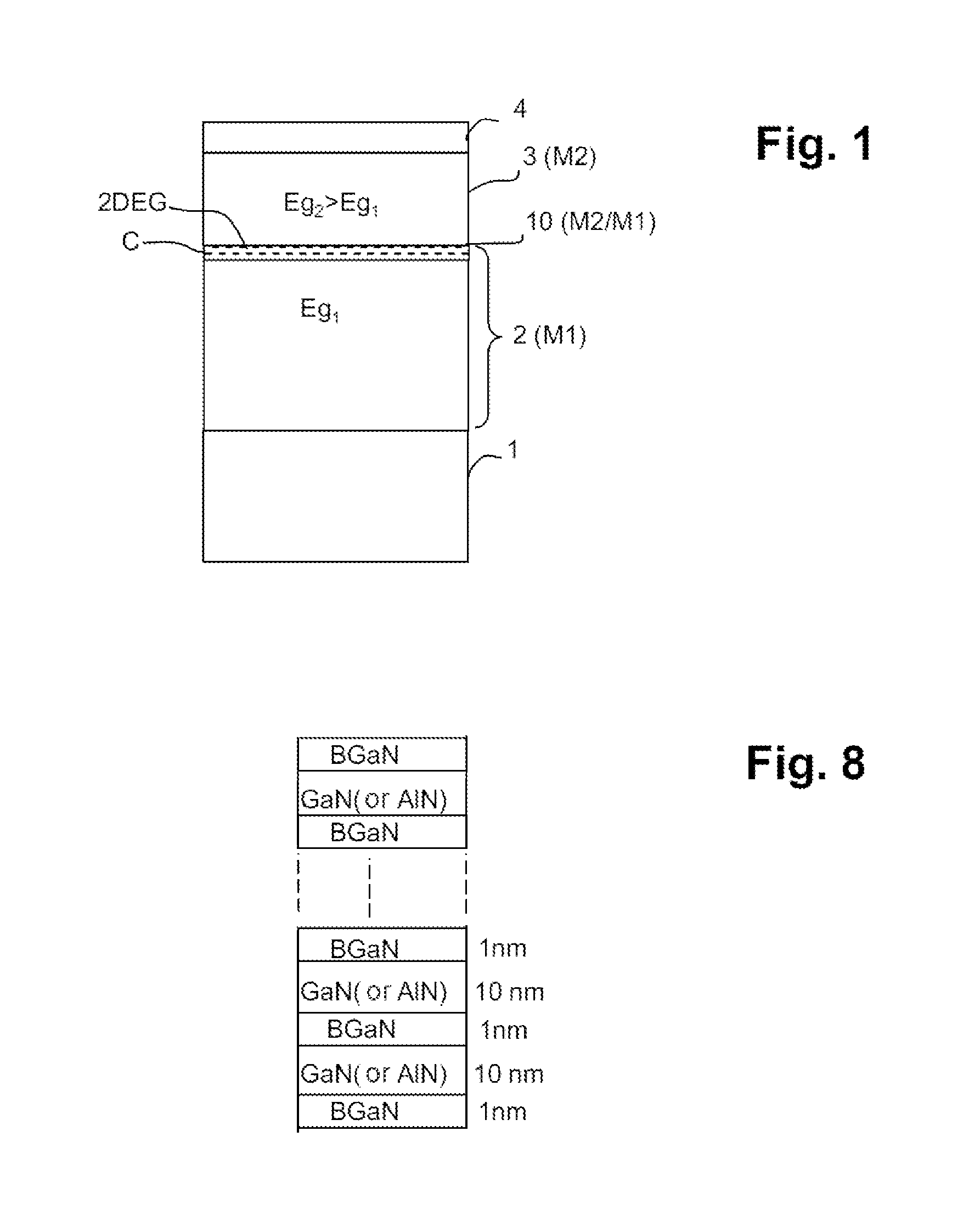
[0049]According to the invention, the structure comprises a BGaN layer in the buffer layer, under the channel.

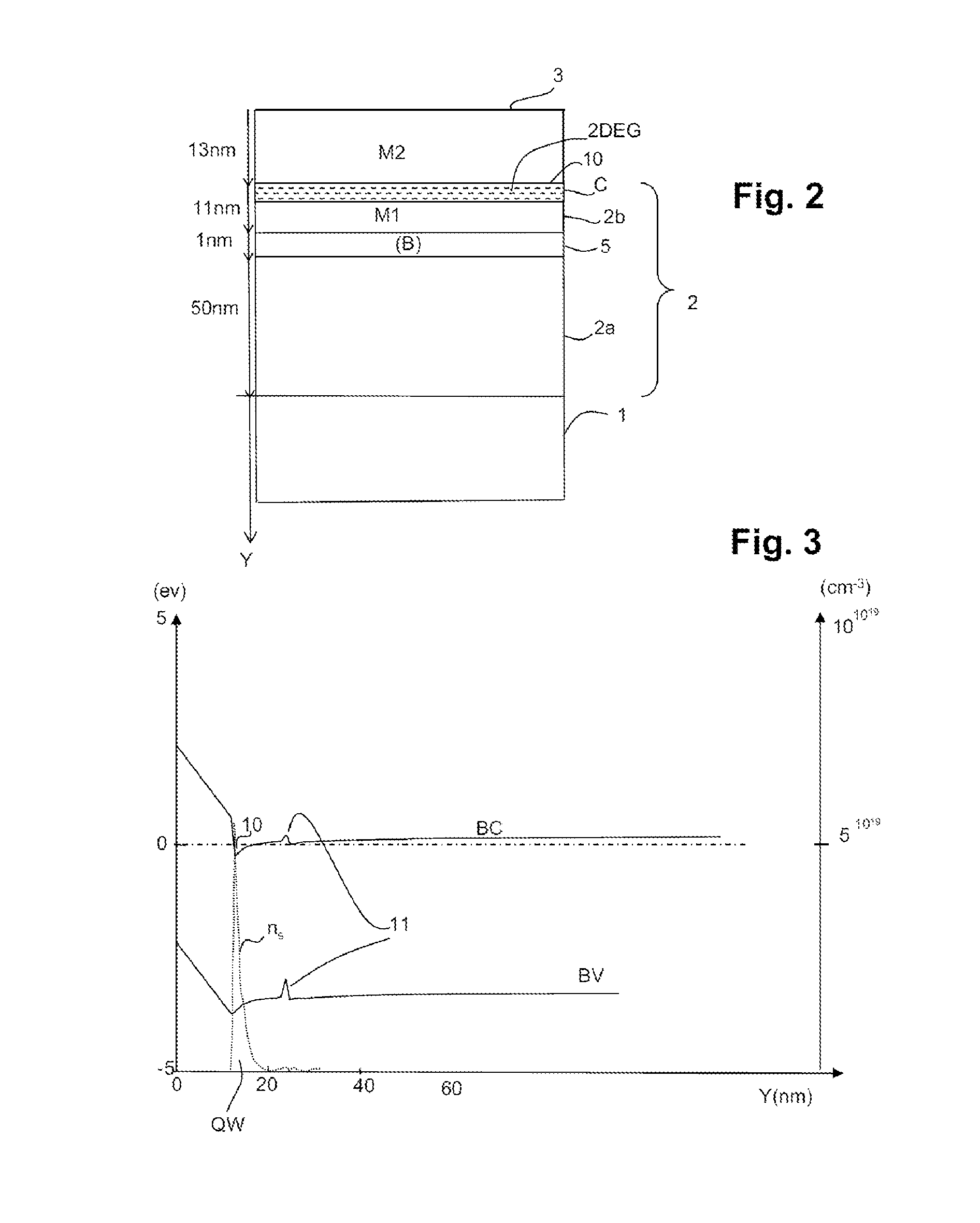
[0050]A first example of an electronic structure according to the invention is illustrated in FIG. 2. It comprises the following stack of layers, in the order th...


PUM


Abstract

An electronic HEMT transistor structure comprises a heterojunction formed from a first layer, called a buffer layer, of a first wide bandgap semiconductor material, and a second layer of a second wide bandgap semiconductor material, with a bandgap width EG.sub.2 larger than that Eg.sub.1 of the first material, and a two-dimensional electron gas flowing in a channel confined in the first layer under the interface of the heterojunction. The first layer furthermore comprises a layer of a BGaN material under the channel, with an average boron concentration of at least 0.1%, improving the electrical performance of the transistor. Application to microwave power components.

Description

FIELD OF THE INVENTION[0001]The invention relates to a so-called HEMT (high electron mobility transistor) electronic heterojunction field-effect transistor structure based on heterostructures formed from wide bandgap semiconductor materials, so-called wide-gap materials.DESCRIPTION OF THE PRIOR ART[0002]Wide bandgap semiconductor materials are semiconductor materials that have a bandgap width wider than about 2 eV, corresponding to the domain of micron-sized wavelengths, from the near infrared to the deep UV. They typically comprise nitrides of group-III elements, but also diamond and oxides such as zinc oxide.[0003]A group-III nitride is a composition of one or more elements from column III, for example B, Al, Ga or In, alloyed with nitrogen N (group V element). They include binary compositions such as GaN, AlN, BN; or ternary alloys, comprising two group-III elements, such as AlxGa1-xN, InxAl1-xN, BxGa1-xN, BxAl1-xN, quaternary alloys comprising 3 group-III elements, BxAlyGa1-x-yN...

Claims


Application Information

Patent Timeline
Patent Type & Authority Applications(United States)
IPC IPC(8): H01L29/778H01L29/205
CPCH01L29/205H01L29/7787H01L21/0237H01L21/02458H01L21/02502H01L21/02507H01L21/0254H01L23/291H01L23/3171H01L29/04H01L29/1075H01L29/2003H01L29/201H01L29/7783H01L2924/0002
Inventor OUGAZZADEN, ABDALLAHPOISSON, MARIE-ANTOINETTERAVINDRAN, VINODSOLTANI, ALIDE JAEGER, JEAN-CLAUDE
Owner THALES SA
Why Eureka
Try Eureka