
Switching power supply apparatus and semiconductor device

Active Publication Date: 2014-11-06
PANASONIC SEMICON SOLUTIONS CO LTD
View PDF6 Cites 49 Cited by
  • Summary
  • Abstract
  • Description
  • Claims
  • Application Information

AI Technical Summary

Benefits of technology

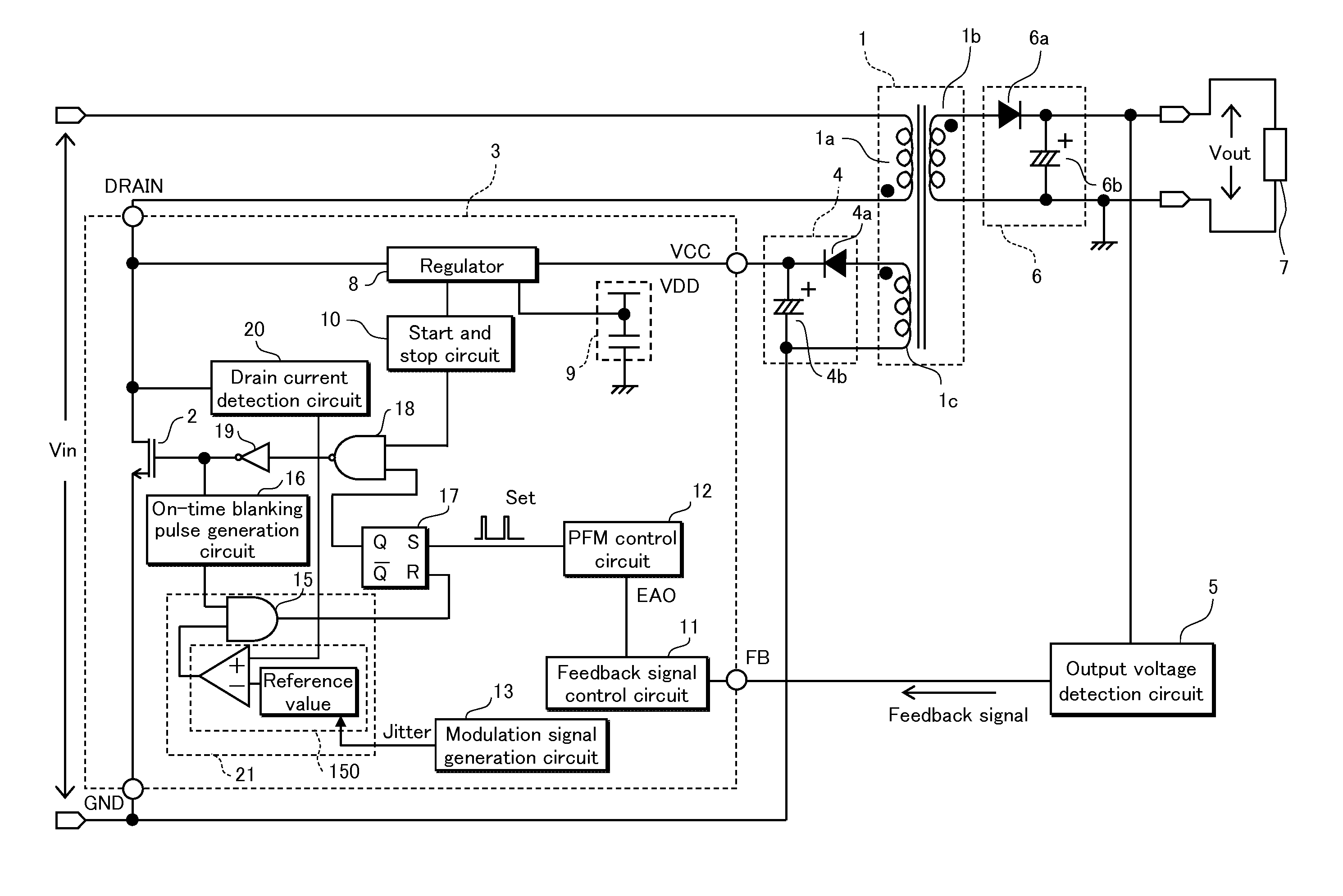
The present disclosure describes a switching power supply apparatus that can modulate its switching frequency to reduce noise and prevent the generation of sound. This is achieved by diffusing the energy of the switching frequency and its harmonic frequencies, which decreases the peak value of the noise. The apparatus also performs input control separately for the switching frequency and the modulation signal to ensure stable modulation effects and reduce noise. Overall, the apparatus allows for a wide operating frequency range and eliminates the need for special measures against sound generation, such as adhering to transformers or impregnating them. Additionally, the apparatus can modify its switching frequency in response to changes in load or output requirements, leading to increased effectiveness and efficiency.

Problems solved by technology

Generally, in a light load state such as the standby mode or the like, a dominant energy loss in a switching power supply apparatus is a switching loss due to a switching operation.
This causes a problem that spectral components of a high-frequency current flowing through the switching element concentrate in the switching frequency and its harmonic components, and as a result noise (electrical noise) easily occurs.
Components such as filter circuits against the noise are necessary, and this hinders size-reduction and cost-reduction of the switching power supply apparatus.
Here, the terminal noise represents a leakage voltage that is induced due to leakage of a switching frequency by a switching operation and harmonic components thereof from a commercial AC power supply to the outside.
This results in increase in switching loss to hinder improvement of power efficiency.
However, these measures cause increase in area of circuits, increase in cost, and so on.

Method used


Image

  • Switching power supply apparatus and semiconductor device
  • Switching power supply apparatus and semiconductor device
  • Switching power supply apparatus and semiconductor device

Examples


embodiment 1

Modifications of Embodiment 1

Modification 1

[0128]A switching power supply apparatus relating to Modification 1 of Embodiment 1 is substantially the same as the switching power supply apparatus relating to Embodiment 1, except for a method of modulating the peak value of the current flowing through the switching element.

[0129]FIG. 8 is a circuit diagram of a turn-off control circuit 150 relating to Modification 1 of Embodiment 1. Reference numerals 151, 156, and 157 each represent an inverter circuit, reference numeral 152 represents a constant current source, reference numeral 153 represents a P-MOSFET, reference numerals 154, 158, and 159 each represent an N-MOSFET, and reference numeral 155 represents a smoothing capacitor. The N-MOSFETs 158 and 159 constitute a mirror circuit.

[0130]In the turn-off control circuit 150 relating to Embodiment 1, the peak value of the current flowing through the switching element 2 is modulated by modulating the reference voltage input as a voltage a...

modification 2

[0147]FIG. 9 is a circuit diagram of a turn-off control circuit 150 relating to Modification 2 of Embodiment 1.

[0148]The turn-off control circuit 150 adds a current for charging a capacitor of a delay time generation circuit 160 and a current corresponding to a current signal Jitter which is output from a modulation signal generation circuit 13, thereby to modulate a delay time.

modification 3

[0149]FIG. 10 is a circuit diagram of a turn-off control circuit 150 relating to Modification 3 of Embodiment 1.

[0150]The turn-off control circuit 150 modulates an output signal Vis of a drain current detection circuit 20 which is input as a voltage of a plus side of a comparator 14, thereby to modulate a peak value of a current flowing through a switching element 2. The operating principle of modulation is substantially the same as that of Embodiment 1, and accordingly detailed description thereof is omitted here.

[0151]The switching power supply apparatus relating to Modification 3 of Embodiment 1 exhibits substantially the same effects as those of the switching power supply apparatuses relating to Embodiment 1 and Modifications 1 and 2 of Embodiment 1.


PUM


Abstract

A switching power supply apparatus includes a PFM control circuit that outputs a clock signal Set such that a switching frequency of a switching element varies in accordance with a load state. The clock signal Set determines a turn-on timing of the switching element. A reference value of a current flowing through the switching element determines a turn-off timing of the switching element. A modulation signal is applied to the turn-off timing of the switching element to modulate one of a peak value of a drain current flowing through the switching element and an on-time of the switching element. Input control is performed separately on the clock signal Set and the modulation signal. Accordingly, even when the clock signal Set and the modulation signal contribute to each other to offset each other, modulation effects are not cancelled.

Description

CROSS REFERENCE TO RELATED APPLICATION[0001]This is a continuation application of PCT Application No. PCT / JP2012 / 004676 filed Jul. 24, 2012, designating the United States of America, which in turn claims the benefit of Japanese Application No. 2011-258908, filed on Nov. 28, 2011, the disclosures of which, including the specification, drawings and claims, is incorporated herein by reference in their entirety.TECHNICAL FIELD[0002]The present disclosure relates to a switching power supply apparatus that performs switching on an input voltage through a switching element to control an output voltage, and to a semiconductor device that constitutes the switching power supply apparatus.BACKGROUND ART[0003]Conventionally, as a power supply apparatus for general appliances for household use such as home electric appliances, a switching power supply apparatus has been widely used that includes a semiconductor device controlling an output voltage with use of a switching operation of a semicondu...

Claims


Application Information

Patent Timeline
IPC IPC(8): H02M3/335
CPCH02M3/33507H02M1/44H02M3/33515H02M3/33546H02M3/33576H02M3/3372H02M3/3384
Inventor TAKAHASHI, KENSUKESAJI, TAKASHI
Owner PANASONIC SEMICON SOLUTIONS CO LTD
Learn More