Semiconductor device and high-frequency module

a technology of semiconductor devices and high-frequency modules, applied in the direction of electrical apparatus interference reduction, radio transmission, electrical apparatus, etc., can solve the problems of long development time, immense development cost, intermodulation distortion, etc., and achieve the effect of reducing intermodulation distortion

Active Publication Date: 2014-11-06
MURATA MFG CO LTD
View PDF1 Cites 6 Cited by
  • Summary
  • Abstract
  • Description
  • Claims
  • Application Information

AI Technical Summary

Benefits of technology

[0011]An effect obtained from the representative aspect of the present invention disclosed in this description will be described below in brief.
[0012]That is, it is possible to further reduce intermodulation distortion.

Problems solved by technology

However, the gate resistor is a semiconductor resistor formed of a semiconductor integrated circuit and thus is a nonlinear resistor.
Since the gate resistors of the HEMTs of the high-frequency switch which is turned off are unevenly supplied with a leaking RF signal, there can be intermodulation distortion.
However, new development requires a long development time and immense development costs and thus is not realistic.
However, an increase in resistance causes an increase in chip area and chip cost.

Method used


Image

  • Semiconductor device and high-frequency module
  • Semiconductor device and high-frequency module
  • Semiconductor device and high-frequency module

Examples


Embodiment Construction

[0024]First, a summary of representative embodiments of the present invention disclosed in this application will be described below. Reference signs of the drawings written in parentheses in the summary of the representative embodiments merely represent that an element having a reference sign attached thereto belongs to the concept of the corresponding element.

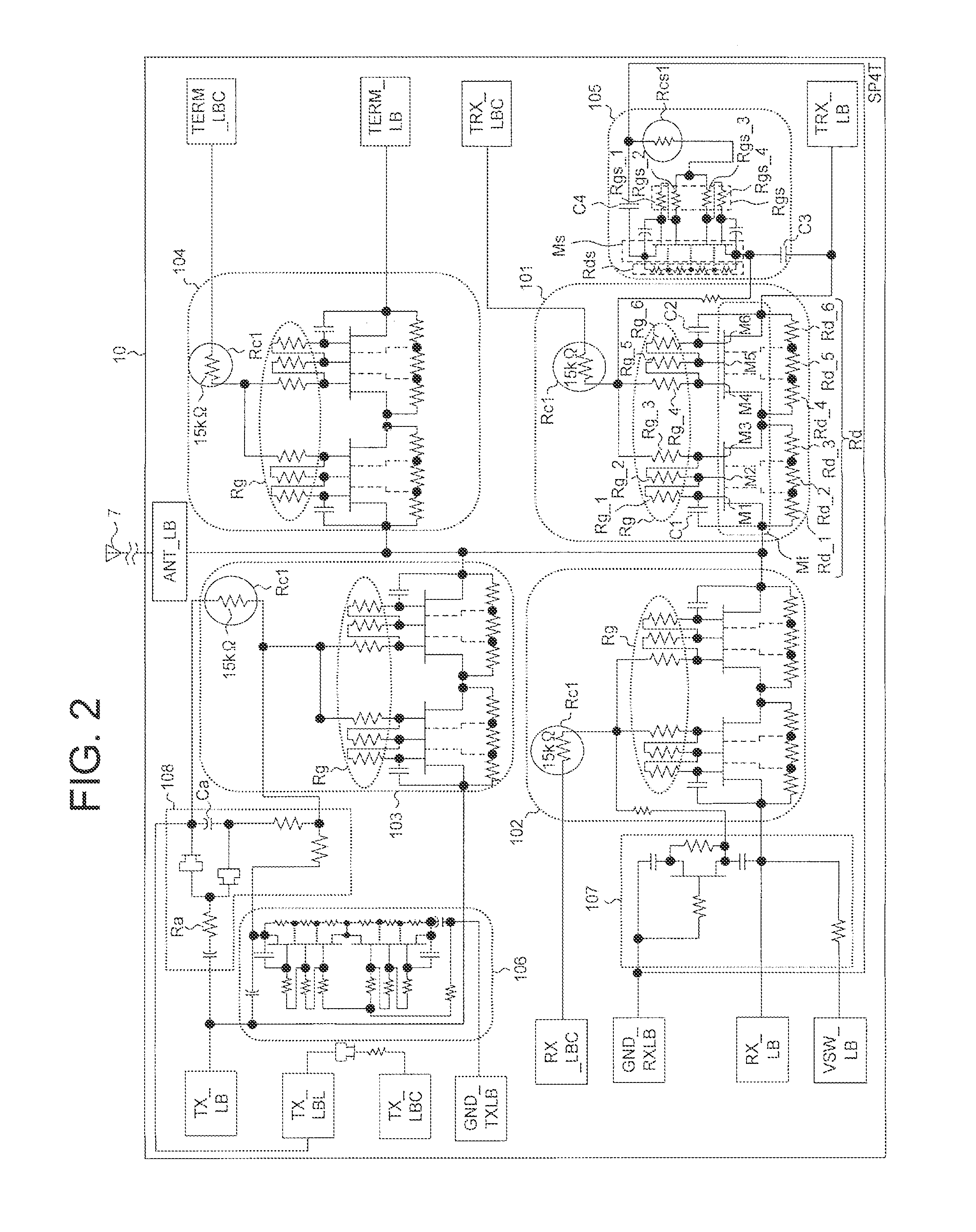
[1] (A Resistor Having High Linearity is Used as a Coupling Resistor in a Switch of an FDD Transceiving Terminal)

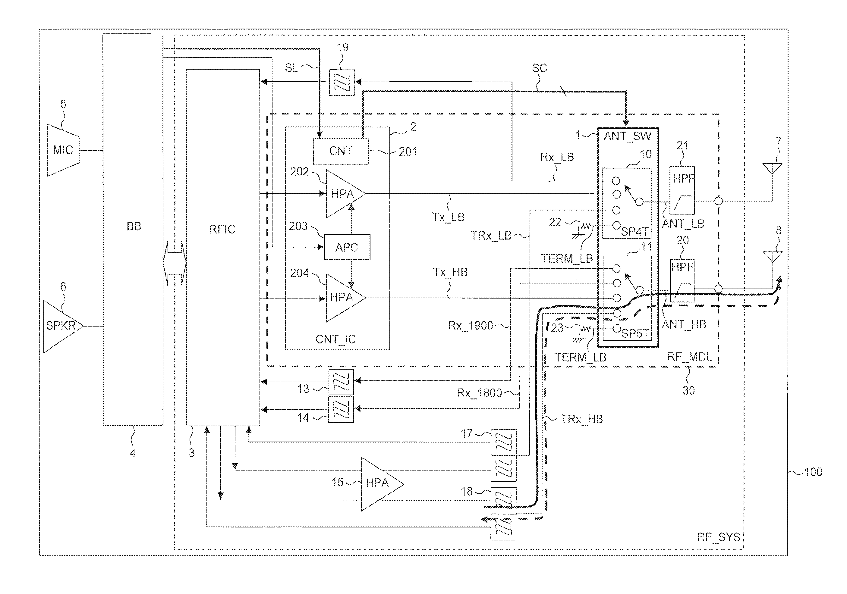
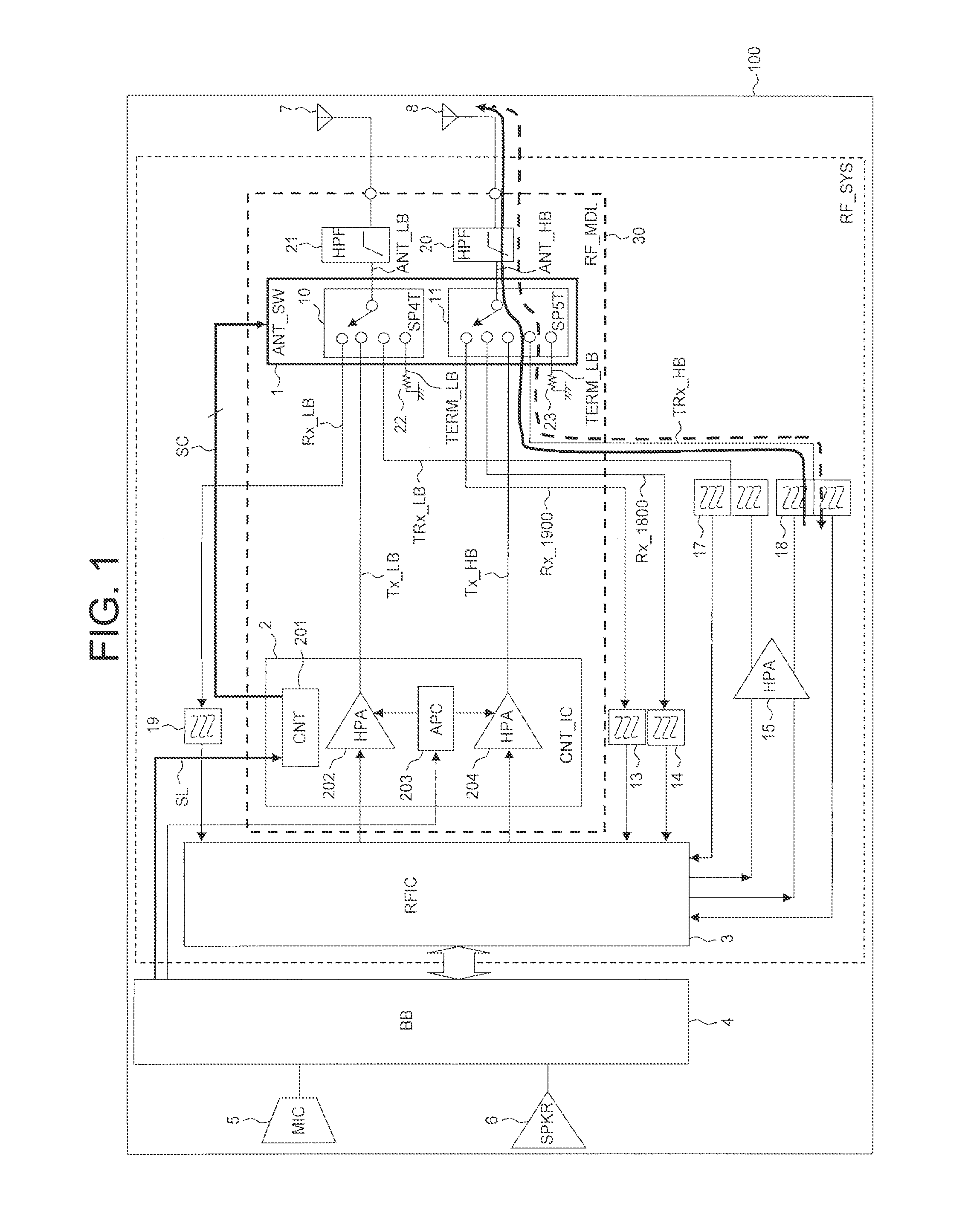
[0025]A semiconductor device (1) according to a representative embodiment of the present invention includes: an antenna terminal (ANT_LB, ANT_HB) that is connected to an antenna (7, 8); plural external terminals (TRX_LB, TX_LB, RX_LB, TERM_LB, TRX_HB, TX_HB, RX—1800, RX—1900, TERM_HB) that are supplied with an RF signal; plural first high-frequency switches (101 to 104, 111 to 114) that are disposed between the antenna terminal and the external terminals; and plural control terminals (TRX_LBC, TX_LBC, RX_LBC, TERM_L...


PUM


Abstract

Reduction of intermodulation distortion in a high-frequency switch is achieved. A semiconductor device (1) includes an antenna terminal (ANT_LB), plural external terminals (RX_LB, TX_LB, TRX_LB, TERM_LB), plural first high-frequency switches (101 to 104), and plural control terminals. Each first high-frequency switch includes plural first field-effect transistors, plural first resistors (Rg1 to Rg6) connected to the gate terminals of the first field-effect transistors, and a second resistor (Rc) disposed between the corresponding control terminal and the first resistors. The second resistor in the first high-frequency switch disposed between the first terminal supplied with an RF transmission signal and an RF reception signal of a frequency division duplex system and the antenna terminal is configured so that linearity of current-voltage characteristics thereof is higher than linearity of current-voltage characteristics of the first resistor.

Description

TECHNICAL FIELD[0001]The present invention relates to a semiconductor device having incorporated therein an antenna switch for a wireless communication system and a high-frequency module having the semiconductor device incorporated therein, and more particularly, to an effective technique of reducing intermodulation distortion in an antenna switch.BACKGROUND ART[0002]Recently, in the field of mobile phones, markets for third-generation mobile phones of a wideband-code division multiple access (W-CDMA) system in addition to a global system for mobile communications (GSM) (registered trademark) system have rapidly grown. The W-CDMA system is a frequency division duplex (FDD) communication system in which a frequency band is divided into a frequency band for a transmission signal and a frequency band for a reception signal to simultaneously perform transmission and reception, unlike the GSM system. A signal path through which signals of different frequencies are simultaneously transmit...

Claims


Application Information

Patent Timeline
Patent Type & Authority Applications(United States)
IPC IPC(8): H04B1/52H04B1/44
CPCH04B1/525H04B1/44H04B1/0064H04B15/04
Inventor TANGE, EIGOKOYA, SHIGEKISHIGENO, YASUSHINAKAJIMA, AKISHIGE
Owner MURATA MFG CO LTD
Why Eureka
Try Eureka