In-cell OLED touch display panel structure

Active Publication Date: 2014-11-27
SUPERC TOUCH CORP
View PDF6 Cites 22 Cited by
  • Summary
  • Abstract
  • Description
  • Claims
  • Application Information

AI Technical Summary

Benefits of technology

[0014]The object of the present invention is to provide an in-cell OLED touch display panel structure capable of significantly decre

Problems solved by technology

Such well known skill of the touch panel may increase additional weight and thickness of the touch display panel, and may further reduce the light penetration rate, and increase reflectance and haze of the touch display panel.
For the on-cell touch technology, it needs a sensing layer to be

Method used


Image

  • In-cell OLED touch display panel structure
  • In-cell OLED touch display panel structure
  • In-cell OLED touch display panel structure

Examples


Embodiment Construction

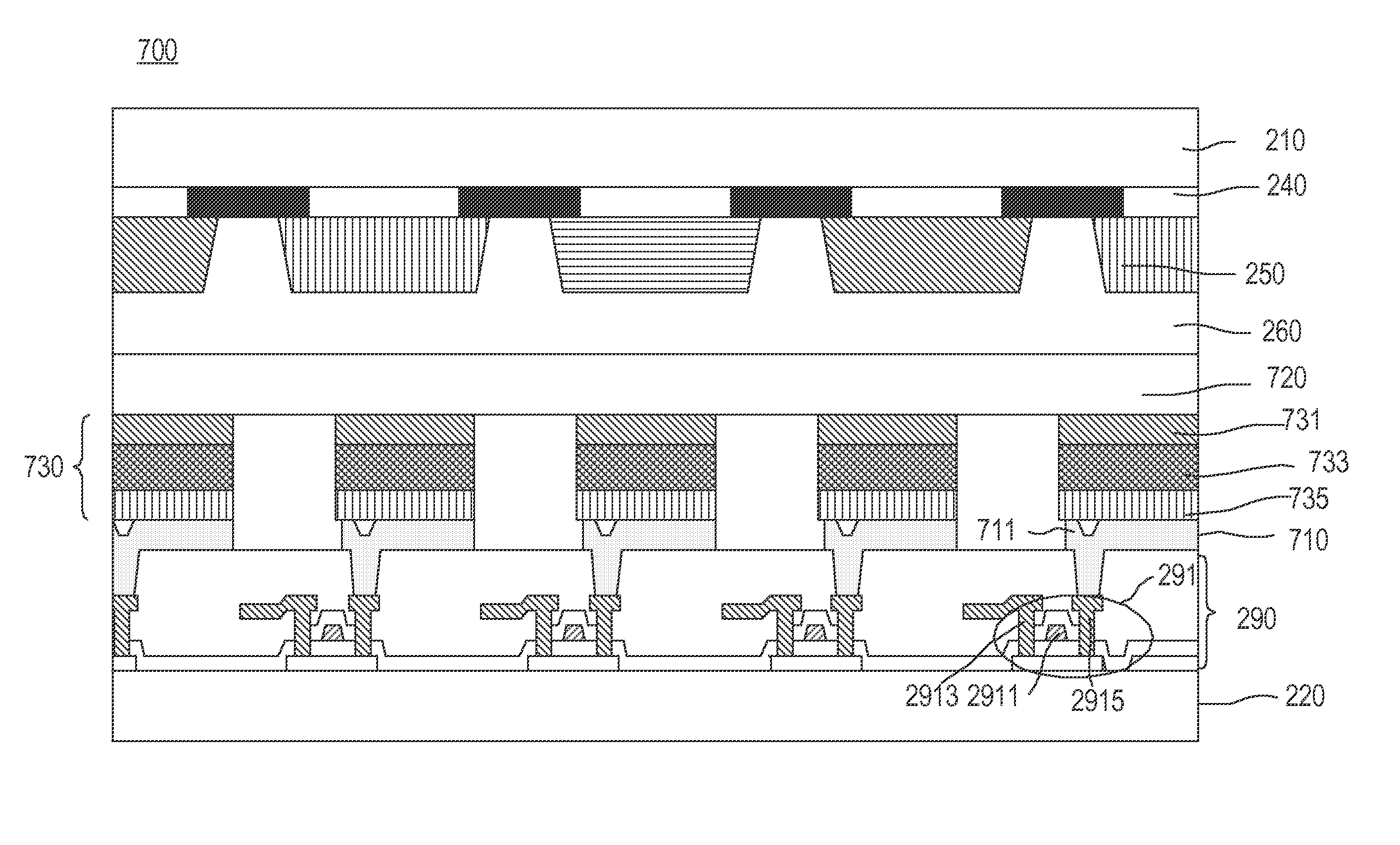
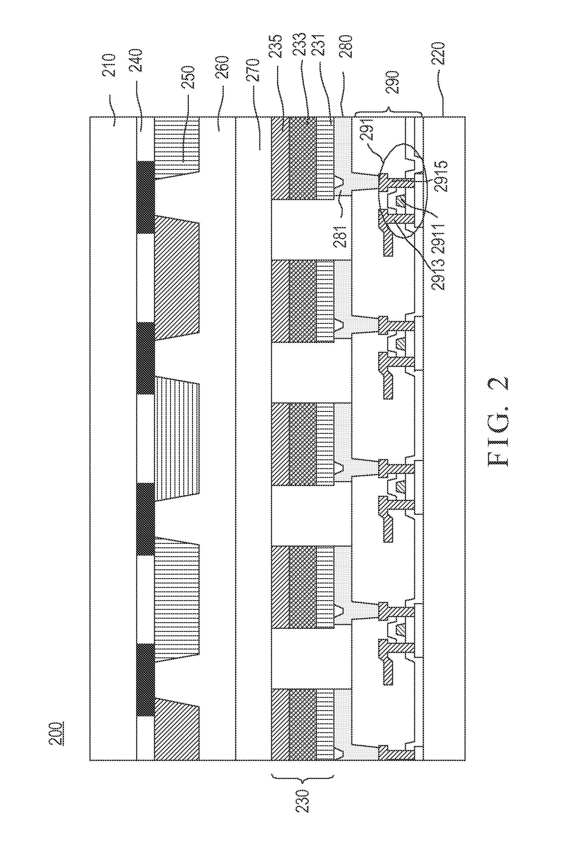
[0023]FIG. 2 is the stack-up diagram of an in-cell OLED touch display panel structure 200 in accordance with the present invention. As shown, the in-cell OLED touch display panel structure 200 includes an upper substrate 210, a lower substrate 220, an OLED layer 230, a black matrix layer 240, a color filter layer 250, an over coating layer 260, a cathode layer 270, an anode layer 280, and a thin film transistor (TFT) layer 290.

[0024]The upper substrate 210 and the lower substrate 220 are preferably glass substrates or plastic substrates, and are parallel to each other. The OLED layer 230 is disposed between the upper and lower substrates 210, 220.

[0025]The black matrix layer 240 is disposed at one surface of the upper substrate 210 that faces the OLED layer 230, and the black matrix layer 240 is composed of a plurality of opaque conductor lines.

[0026]FIG. 3 shows a prior black matrix layer. As shown in FIG. 3, the prior black matrix layer is composed of lines of insulating material ...


PUM


Abstract

An in-cell OLED touch display panel structure includes an upper substrate, a lower substrate, an OLED layer configured between the upper and lower substrates, and a black matrix layer. The black matrix layer is disposed at one surface of the upper substrate that faces the OLED layer, and the black matrix layer is composed of a plurality of opaque conductor lines. The plurality of opaque conductor lines is divided into a first group of opaque conductor lines, a second group of opaque conductor lines, and a third group of opaque conductor lines. The second group of opaque conductor lines is formed with N mesh-like polygonal regions. The opaque conductor lines in any one of the polygonal regions are electrically connected together, while any two polygonal regions are not connected, so as to form a single-layered touch sensing pattern on the black matrix layer.

Description

CROSS REFERENCE TO RELATED APPLICATION[0001]This application claims the benefits of the Taiwan Patent Application Serial Number 102215172, filed on Aug. 13, 2013, the subject matter of which is incorporated herein by reference.[0002]This application is a continuation-in-part (CIP) of U.S. Patent application for an “in-cell touch display panel structure”, U.S. app. Ser. No. 13 / 795,788, filed on Mar. 12, 2013.BACKGROUND OF THE INVENTION[0003]1. Field of the Invention[0004]The present invention relates to a structure of touch display panel and, more particularly, to an in-cell OLED touch display panel structure.[0005]2. Description of Related Art[0006]Among many types of flat panel displays, the organic light emitting diode display (OLED) technology is the one with great potential. OLED was first published by Eastman Kodak Co. in 1987. It has the features of thinness, light weight, self-illumination, low driving voltage, high efficiency, high contrast, high color saturation, fast respo...

Claims


Application Information

Patent Timeline
IPC IPC(8): H01L27/32
CPCH01L27/3276H01L27/323G06F3/0412G06F3/0443G06F3/0448H10K59/40H10K50/865
Inventor LEE, HSIANG-YU
Owner SUPERC TOUCH CORP
Why Eureka
Try Eureka