Fast testing switch device and the corresponding tft-lcd array substrate

a switch device and array substrate technology, applied in semiconductor/solid-state device testing/measurement, semiconductor/solid-state device details, instruments, etc., can solve the problems of high cost, large space occupation, and inability to achieve narrow-bezel design, so as to achieve enhanced tft-lcd array substrate yield rate and avoid crosstalk

Active Publication Date: 2015-01-15
SHENZHEN CHINA STAR OPTOELECTRONICS TECH CO LTD
View PDF9 Cites 10 Cited by
  • Summary
  • Abstract
  • Description
  • Claims
  • Application Information

AI Technical Summary

Benefits of technology

[0028]The fast testing switch device includes at least two switch TFTs. When the liquid crystal panel including the TFT-LCD array substrate is in its normal operation, the data line or gate line of th...

Problems solved by technology

However, the shorting bar not only results in high cost but also oc...

Method used


Image

  • Fast testing switch device and the corresponding tft-lcd array substrate
  • Fast testing switch device and the corresponding tft-lcd array substrate
  • Fast testing switch device and the corresponding tft-lcd array substrate

Examples


Embodiment Construction

[0033]Embodiments of the invention will now be described more fully hereinafter with reference to the accompanying drawings, in which embodiments of the invention are shown.

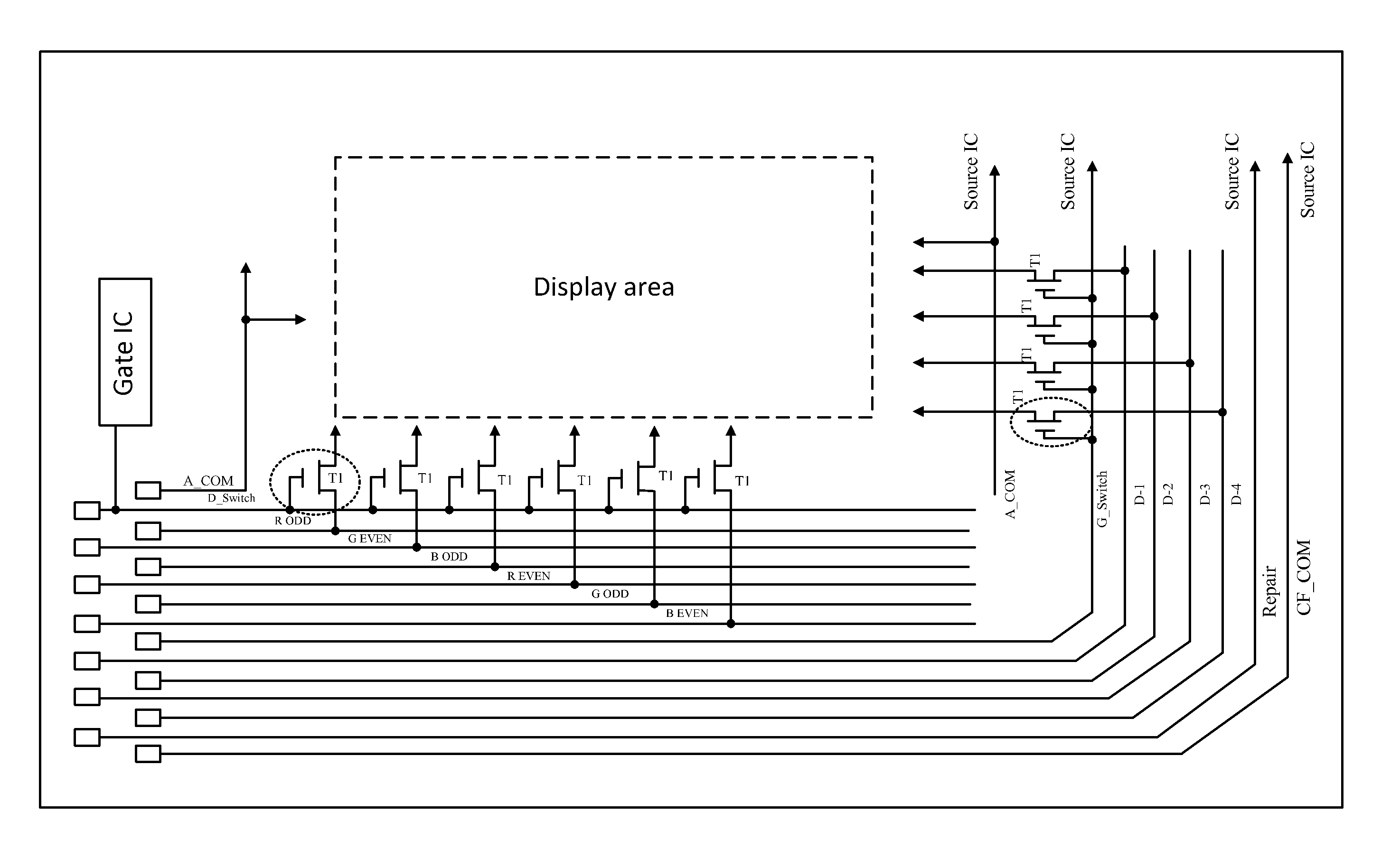
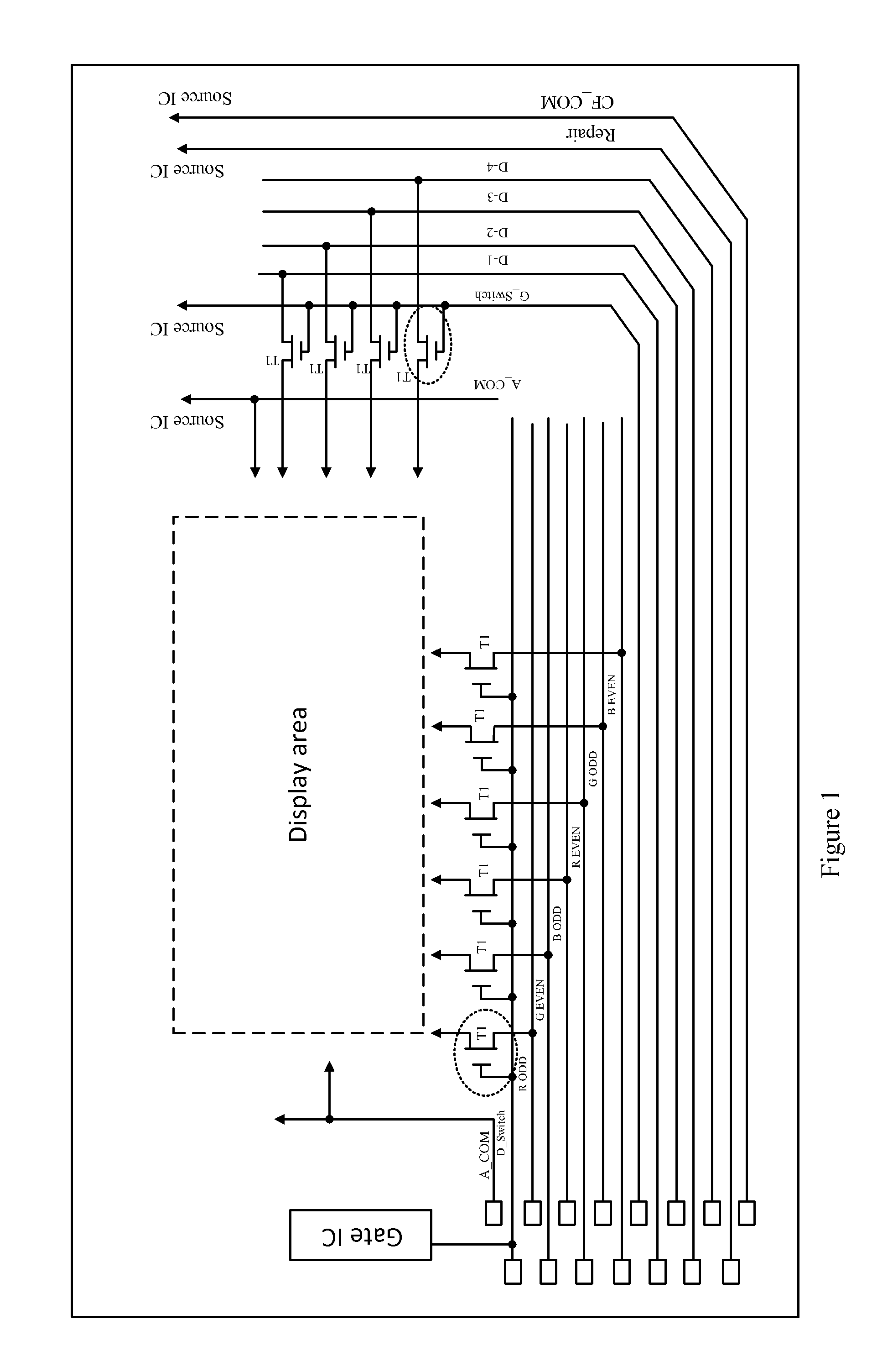
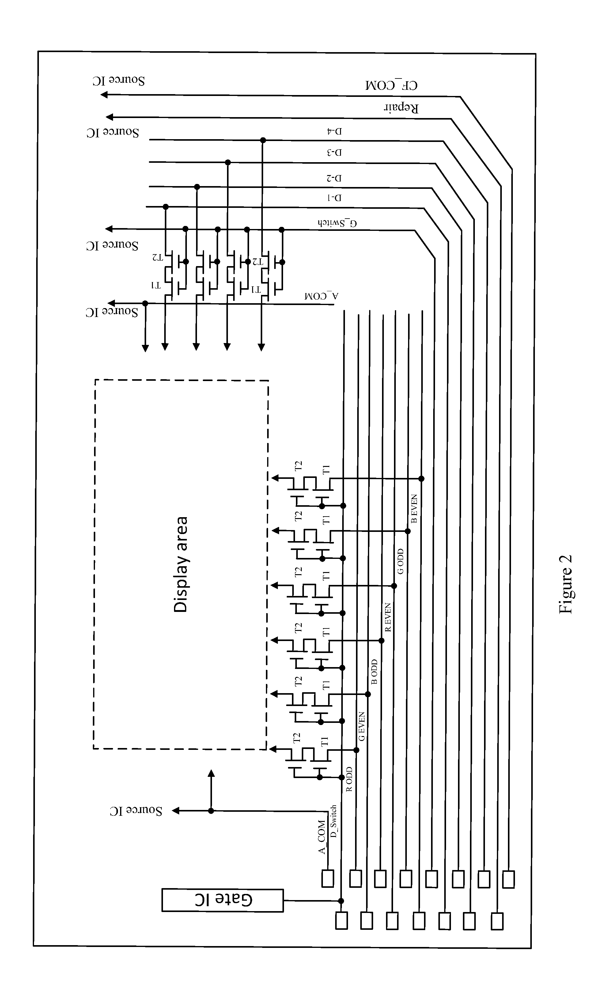
[0034]FIG. 1 is a schematic view of a TFT-LCD array substrate in accordance with one embodiment. In the embodiment, the TFT-LCD array substrate includes a display area and a peripheral area surrounding the display area. The display area includes a plurality of gate lines and data lines connecting to the TFTs arranged within the display area. Specifically, the display area includes a plurality of gate lines and data lines vertical to each other. Each of the intersection of the data lines and gate lines connects to one TFT unit. Each of the TFT unit includes a TFT, a liquid crystal capacitor, and a storage capacitor. A source of the TFT connects to the data line, and a gate of the TFT connects to the gate line. The configuration of the data lines, gate lines, and TFT units in the display areas are general and thus ...


PUM


Abstract

A fast testing switch device arranged on a TFT-LCD array substrate is disclosed. The fast testing switch device switches the testing signals for testing a display area of the TFT-LCD array substrate. The fast testing switch device includes at least a first switch TFT. The gate of the first switch TFT connects to one control chip and a testing block for receiving the switch control signals from the testing block or the turn-off control signals from the control chip. The source of the first switch TFT connects to one data testing line or one gate testing line, and the drain of the first switch TFT connects to the corresponding data line or gate line of the display area. In addition, a corresponding TFT-LCD array substrate is also disclosed. The above configuration not only can achieve the narrow-bezel design but also can enhance the yield rate of the TFT-LCD array substrate.

Description

[0001]This application claims priority to China Patent Application No. 201310288811.1 filed on Jul. 10, 2013 entitled, FAST TESTTING SWITCH DEVICE AND THE CORRESPONDING TFT-LCD ARRAY SUBSTRATE, all of the disclosures of which are incorporated herein by reference in their entirety.BACKGROUND OF THE INVENTION[0002]1. Field of the Invention[0003]Embodiments of the present disclosure relate to Thin Film Transistor-Liquid Crystal Display (TFT-LCD) technology, and more particularly to a fast testing switch device and the corresponding TFT-LCD array substrate.[0004]2. Discussion of the Related Art[0005]In a manufacturing process of TFT-LCD panels, internal circuits have to be tested and fixed upon detecting errors, and this process is called as cell test. Generally, a shorting bar below the gate bonding pad and the source bonding pad is adopted to perform the cell test. After the panel has been tested, the lines of the shorting bar are cut by a laser cut process. However, the shorting bar ...

Claims


Application Information

Patent Timeline
IPC IPC(8): H01L21/66G02F1/1362G02F1/13
CPCG02F2001/136254G02F1/136259G02F1/1309H01L22/34G02F2001/136268G09G3/006G09G2300/0426G02F1/136254G02F1/136268
Inventor LV, QIBIAO
Owner SHENZHEN CHINA STAR OPTOELECTRONICS TECH CO LTD
Why Eureka
Try Eureka