Semiconductor device

a technology of semiconductors and semiconductors, applied in the direction of solid-state devices, instruments, heat measurement, etc., can solve the problems of unusability, cost increase, and inability to operate conventionally used temperature detecting elements such as photodiodes, and achieve the effect of improving assemblability and cost reduction

Active Publication Date: 2015-01-15
MITSUBISHI ELECTRIC CORP
View PDF5 Cites 0 Cited by
  • Summary
  • Abstract
  • Description
  • Claims
  • Application Information

AI Technical Summary

Benefits of technology

[0007]An object of the present invention is to obtain a semiconductor device in which a temperature detecting function o

Problems solved by technology

Consequently, there have been disadvantages in forming a pad portion for transmitting and receiving a signal between the temperature detecting element and the outside.
This configuration increases a device (chip) area to lead to cost increase, and requires an excessive wire bonding process in the pad portion to impose a greater constraint on assembling of the semiconductor device.
In addition, in a case of a wide ga

Method used


Image

  • Semiconductor device
  • Semiconductor device
  • Semiconductor device

Examples


first preferred embodiment

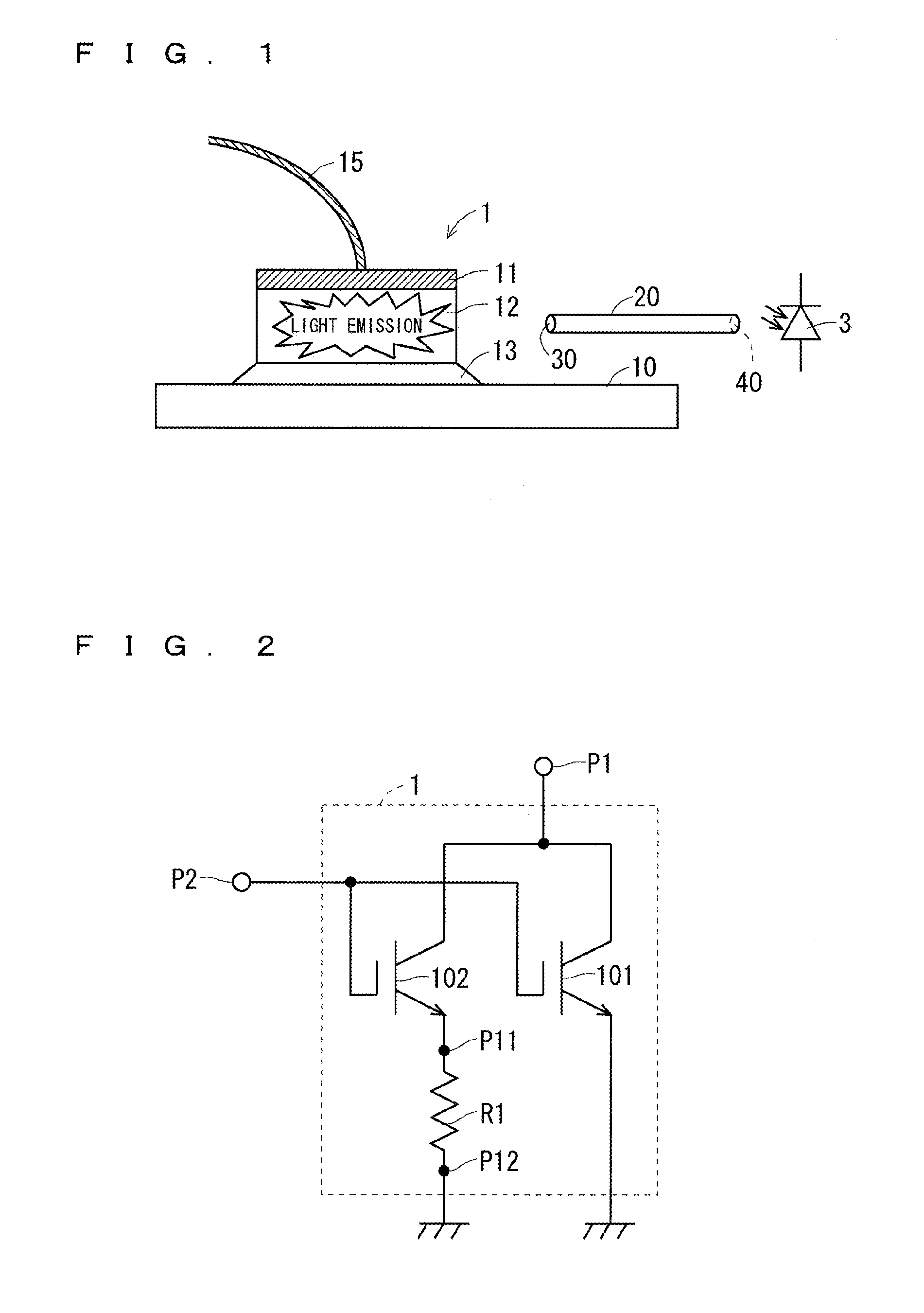
[0028]FIG. 1 is an explanatory view schematically showing a schematic cross-sectional configuration of a semiconductor device according to a first preferred embodiment of the present invention.

[0029]As shown in FIG. 1, a wide gap semiconductor element forming portion 1 is provided on a semiconductor substrate 10. The wide gap semiconductor element forming portion 1 is formed of a laminated structure of a base 13, a semiconductor active portion 12, and an electrode portion 11. From the electrode portion 11 serving as a main electrode portion, a signal can be transmitted to and received from the outside via a signal wire 15.

[0030]FIG. 2 is a circuit diagram showing an example of an internal configuration of the wide gap semiconductor element forming portion 1. As shown in FIG. 2, the wide gap semiconductor element forming portion 1 includes therein an IGBT main body 101 formed of a wide gap semiconductor material having light-emitting property. Further, a current sensing IGBT 102 is p...

second preferred embodiment

[0059]FIG. 6 is an explanatory view schematically showing a planar configuration of a semiconductor device according to a second preferred embodiment of the present invention. As shown in FIG. 6, there are formed a plurality of wide gap semiconductor element forming portions 1a to 1c each of which has an IGBT main body 101, a current sensing IGBT 102, and the like, as shown in FIG. 2. The wide gap semiconductor element forming portions 1a to 1c radiate a plurality (three) of pieces of emitted light from side surfaces of respective semiconductor active portions 12 of the wide gap semiconductor element forming portions 1a to 1c, as shown in FIG. 1, with light emission by the bipolar operation by the respective IGBT main bodies 101 and the like.

[0060]Here, an optical fiber 21 according to the second preferred embodiment is configured by branching parts 21a to 21c having three branches, and an integrated part 21x connected in common to the branching parts 21a to 21c, and is configured s...

third preferred embodiment

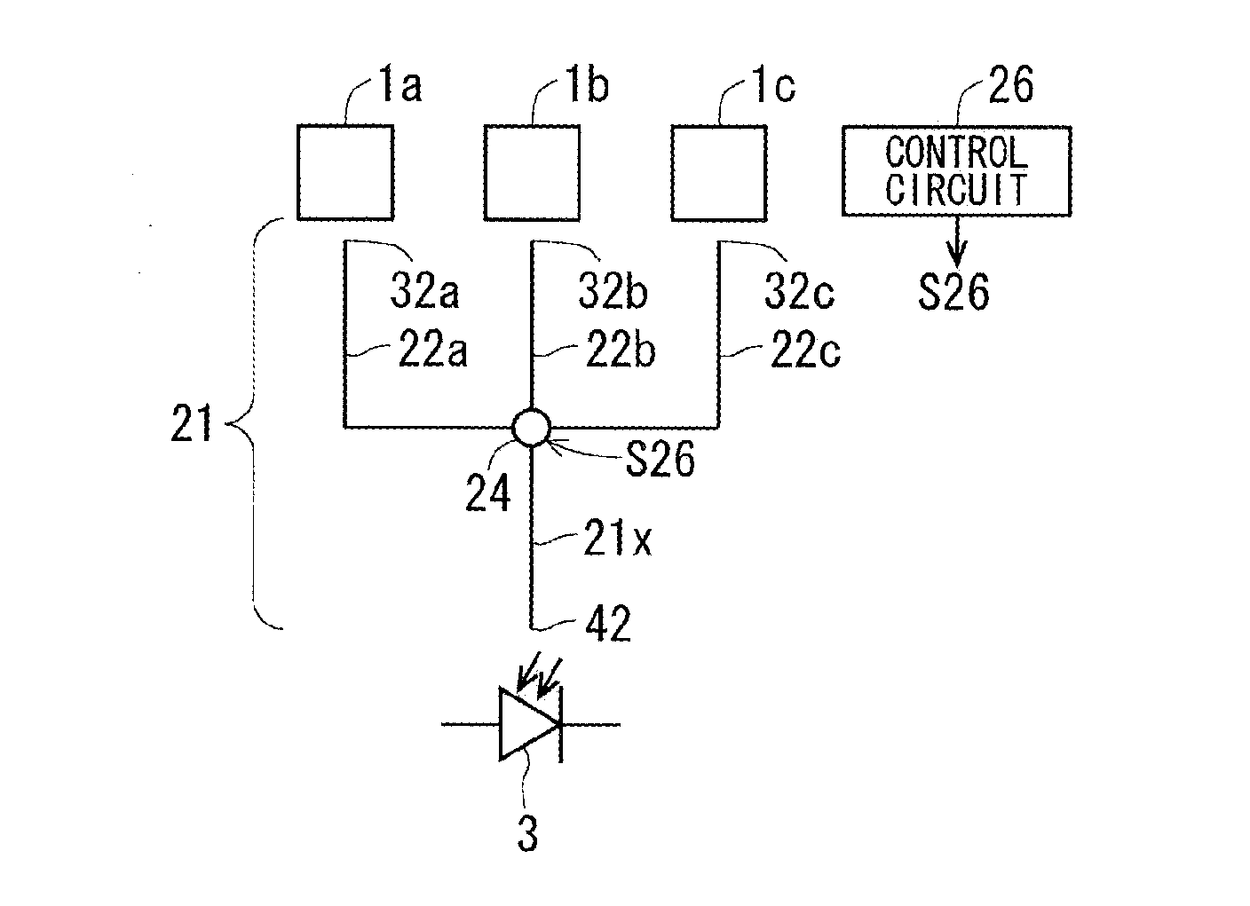
[0067]FIG. 7 is an explanatory view schematically showing a planar configuration of a semiconductor device according to a third preferred embodiment of the present invention. As shown in FIG. 7, the semiconductor device includes a plurality (three) of wide gap semiconductor element forming portions 1a to 1c, corresponding to a wide gap semiconductor element forming portion 1 shown in FIG. 1, in the same manner as in the second preferred embodiment. The wide gap semiconductor element forming portions 1a to 1c emit pieces of light from side surfaces of respective semiconductor active portions 12, as shown in FIG. 1.

[0068]An optical fiber 22 according to the third preferred embodiment is configured by branching parts 22a to 22c having three branches and an integrated part 22x connected in common to the branching parts 22a to 22c, and is provided with a changeover switch 24 serving as an optical path switch between the branching parts 22a to 22c and the integrated part 22x.

[0069]The ch...


PUM


Abstract

An optical fiber is provided between a photodiode and a semiconductor active portion of a wide gap semiconductor element forming portion such that emitted light at the time of light emission of the semiconductor active portion of the wide gap semiconductor element forming portion is incident from an incident surface of the optical fiber, and is received from an emitting surface to the photodiode through the optical fiber. Specifically, the incident surface of the optical fiber is arranged so as to be opposed to a side surface portion of the wide gap semiconductor element forming portion, so that the emitted light at the time of light emission of the wide gap semiconductor element is incident on the incident surface.

Description

BACKGROUND OF THE INVENTION[0001]1. Field of the Invention[0002]The present invention relates to a semiconductor device which has a wide gap semiconductor element and which is capable of detecting a temperature of the wide gap semiconductor element.[0003]2. Description of the Background Art[0004]Conventionally, for measuring an operating temperature of a power semiconductor element, there has been generally used a semiconductor device having a power semiconductor element. The semiconductor device has a temperature detecting element such as a polysilicon diode formed therein electrically independently from the power semiconductor element to detect temperature of the power semiconductor element by temperature characteristics of the temperature detecting element. As a semiconductor device of this type, there is, for example, a current conversion device disclosed in Japanese Patent Application Laid-Open No. 2006-271098.[0005]In a conventional semiconductor device which has a temperature...

Claims


Application Information

Patent Timeline
IPC IPC(8): H01L31/167
CPCH01L31/167H01L2224/48091H01L2224/73265H01L2924/12032G01K7/01G01K2217/00H01L2924/13055H01L2924/00014H01L2924/00
Inventor KAGUCHI, NAOTOTARUI, YOICHIRO
Owner MITSUBISHI ELECTRIC CORP
Why Eureka
Try Eureka