

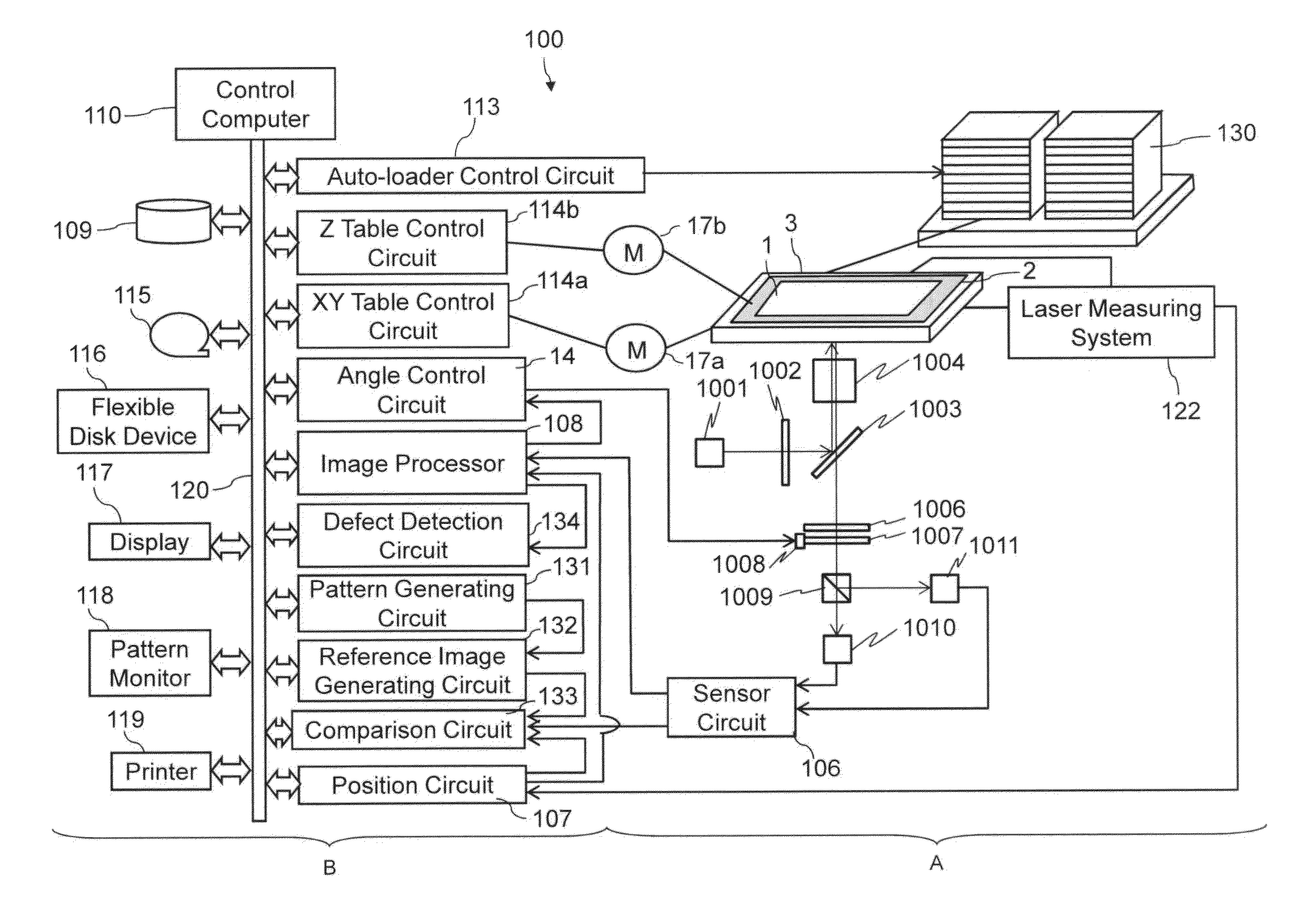
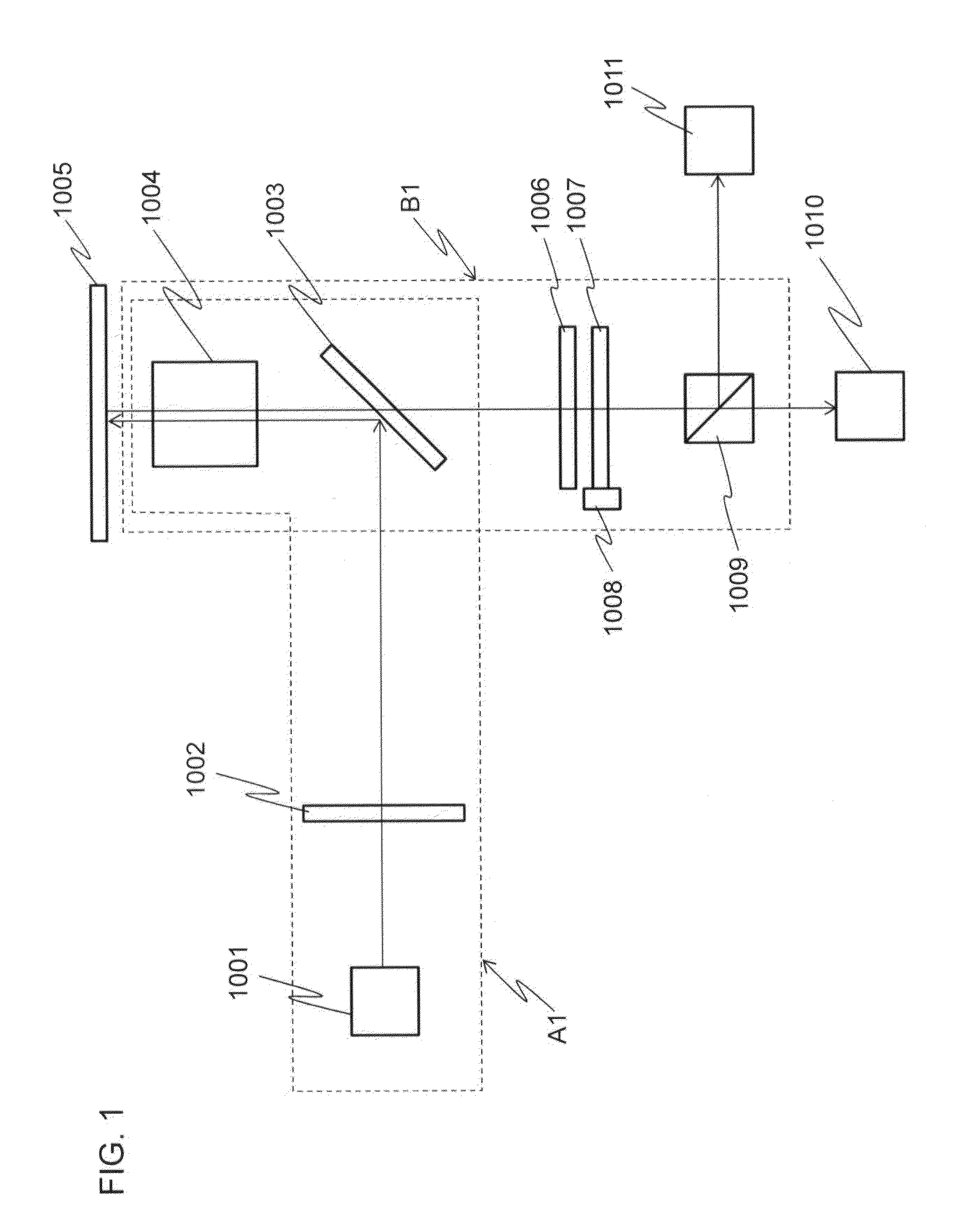
Inspection apparatus
a technology of inspection apparatus and inspection chamber, which is applied in the direction of optical radiation measurement, instruments, polarisation-affecting properties, etc., can solve the problems of reducing the production yield of semiconductor elements, requiring a lot of inspection time, and the light source of eb is not suitable for high throughput inspection process of masks, etc., to achieve the effect of improving resolution performance, enhancing integration degree of semiconductor integrated circuits, and increasing exposure resolution
- Summary
- Abstract
- Description
- Claims
- Application Information
AI Technical Summary
Benefits of technology
Problems solved by technology
Method used
Image

Examples
embodiment 1
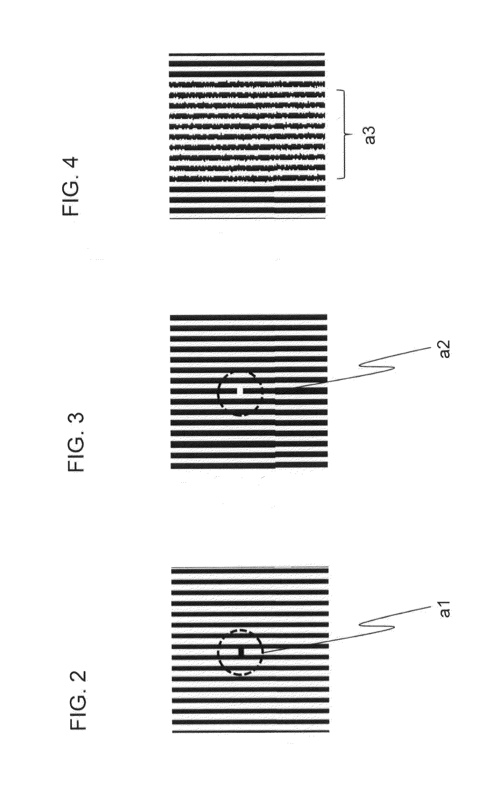
[0038]A short-circuit defect in which lines are short-circuited and an open-circuit defect in which the line is disconnected are detected in a pattern of an optical resolution limit or less. The short-circuit defect and the open-circuit defect have a large influence on a polarization state of illumination light. Therefore, by controlling the polarization state of the illumination light and an optical condition for a polarization control element of an optical system that images light reflected from an inspection target, bright and dark unevenness caused by edge roughness can be removed with the polarization control element thereby extracting only a change in amplitude of the short-circuit defect or open-circuit defect. However, this optical condition is not suitable for the inspection of a region where high contrast is required because a gradation value is lowered both in a white portion and a black portion of an optical image under the optical condition.
[0039]A dimension (Critical D...
embodiment 2
[0066]FIG. 7 illustrates an optical system according to a second embodiment. The optical system of the second embodiment also includes an illumination optical system A2 that illuminates a mask 2005 of the inspection target and an imaging optical system B2 that images the light reflected from the mask 2005 on sensors 2010 and 2011. The illumination optical system A2 includes a light source 2001, a half-wavelength plate 2002, a half mirror 2003, and an objective lens 2004. The imaging optical system B2 includes the objective lens 2004, the half mirror 2003, a half-wavelength plate 2007, a rotation mechanism 2008, and a polarization beamsplitter 2009. The half mirror 2003 and the objective lens 2004 are shared by the illumination optical system A2 and the imaging optical system B2.
[0067]Many patterns provided in the mask 2005 are repetitive patterns such as the line and space pattern, namely, the regular repetitive pattern having the periodicity. For example, the template in the nanoim...
embodiment 3
[0083]FIG. 8 illustrates an example of an optical system according to a third embodiment. The optical system of the third embodiment also includes an illumination optical system A4 that illuminates a mask 3005 of the inspection target and an imaging optical system B3 that images the light reflected from the mask 3005 on the sensors 3010 and 3011.
[0084]The illumination optical system A3 includes a light source 3001, a half-wavelength plate 3015, a Rochon prism 3012 as a branching element, a quarter-wavelength plate 3002, a half mirror 3003, and an objective lens 3004. The imaging optical system B3 includes the objective lens 3004, the half mirror 3003, a quarter-wavelength plate 3007, a polarization beamsplitter 3009 including a rotation mechanism 3013, and a mirror 3014. The half mirror 3003 and the objective lens 3004 are shared by the illumination optical system A3 and the imaging optical system B3.
[0085]Many patterns provided in the mask 3005 are repetitive patterns such as the l...
PUM
| Property | Measurement | Unit |
|---|---|---|
| wavelength | aaaaa | aaaaa |
| width | aaaaa | aaaaa |
| angle | aaaaa | aaaaa |
Abstract
Description
Claims
Application Information