Acidic etching process for si wafers

a technology of acidic surface etching and silicon wafer, which is applied in the manufacture of final products, semiconductor/solid-state devices, basic electric elements, etc., can solve the problems of avoiding the need for extensive cleaning, and achieve the effects of reducing cu findings, reducing roughness, and reducing cos

Inactive Publication Date: 2015-02-12
SOLARWORLD AMERICAS
View PDF10 Cites 18 Cited by
  • Summary
  • Abstract
  • Description
  • Claims
  • Application Information

AI Technical Summary

Benefits of technology

[0010]The present invention is based on the inventor's surprising finding that by contacting at least one surface of a Si wafer as cut with an acidic etching agent metallic and organic contaminants originating from the prior saw process are efficiently removed and the surface roughness can be controlled. ICP-MS results of the acidic etched wafers presented significant lower Cu findings compared to alkaline etched wafers. This result is important regarding the cell degradation. In addition, it has been found that such an etching process obviates the need for extensive cleaning prior to and after the etching step. Accordingly, the present invention allows a fast, cost-efficient process due to less cleaning steps and usage of low grade chemicals for the acidic etching process. Further, the present invention allows to finely tune the amount of roughness of the surface structure of the Si wafer, thus optimizing effectiveness of the passivation layer.
[0011]Accordingly, the same result as in the above-referenced Centaurus process can be achieved alternatively starting with an acidic damage etching process without any ozone or hydrogen peroxide. Selecting for the wafer as cut the acidic single side etching process, followed by the texture etch process after the rear side passivation, reduces the total etch removal by 5-10 μm. This is actually possible only in this etching combination, acidic-alkaline, but not in the combination alkaline-acidic, because the alkaline etching process of wafers as cut affects from begin both sides of the wafer, no matter if it is run in a batch tool or inline tool. The gain in less etch removal is an advantage that helps to improve the production yield as the wafers are cut thinner and thinner.

Problems solved by technology

In addition, it has been found that such an etching process obviates the need for extensive cleaning prior to and after the etching step.

Method used


Image

  • Acidic etching process for si wafers
  • Acidic etching process for si wafers
  • Acidic etching process for si wafers

Examples


example 1

[0049]Monocrystalline wafers obtained by the Czochralski process were contacted with a mixture of AcOH (98 wt.-% in water), HNO3 (69 wt.-% in water), and HF (49 wt.-% in water) as acidic etching agent. The volume ratio of AcOH:HNO3:HF was 10:6:4. The wafers were compared with reference wafers that were processed through the alkaline saw damage etch process, achieving polished surfaces. The quality of the deposited passivation stack was measured comparing the life time and implied Voc in so called “Quasi Tau Samples” using the Sinton photoconductance method that is used for process quality control. Said wafer had a thickness of about 160 μm and were measured at a carrier density of 1E+15. The measured life time was 182 μsec in average for the acidic etched samples, resulting in an implied voltage of 678 mV, while result of the reference samples was 172 μsec in average and also 678 mV.

example 2

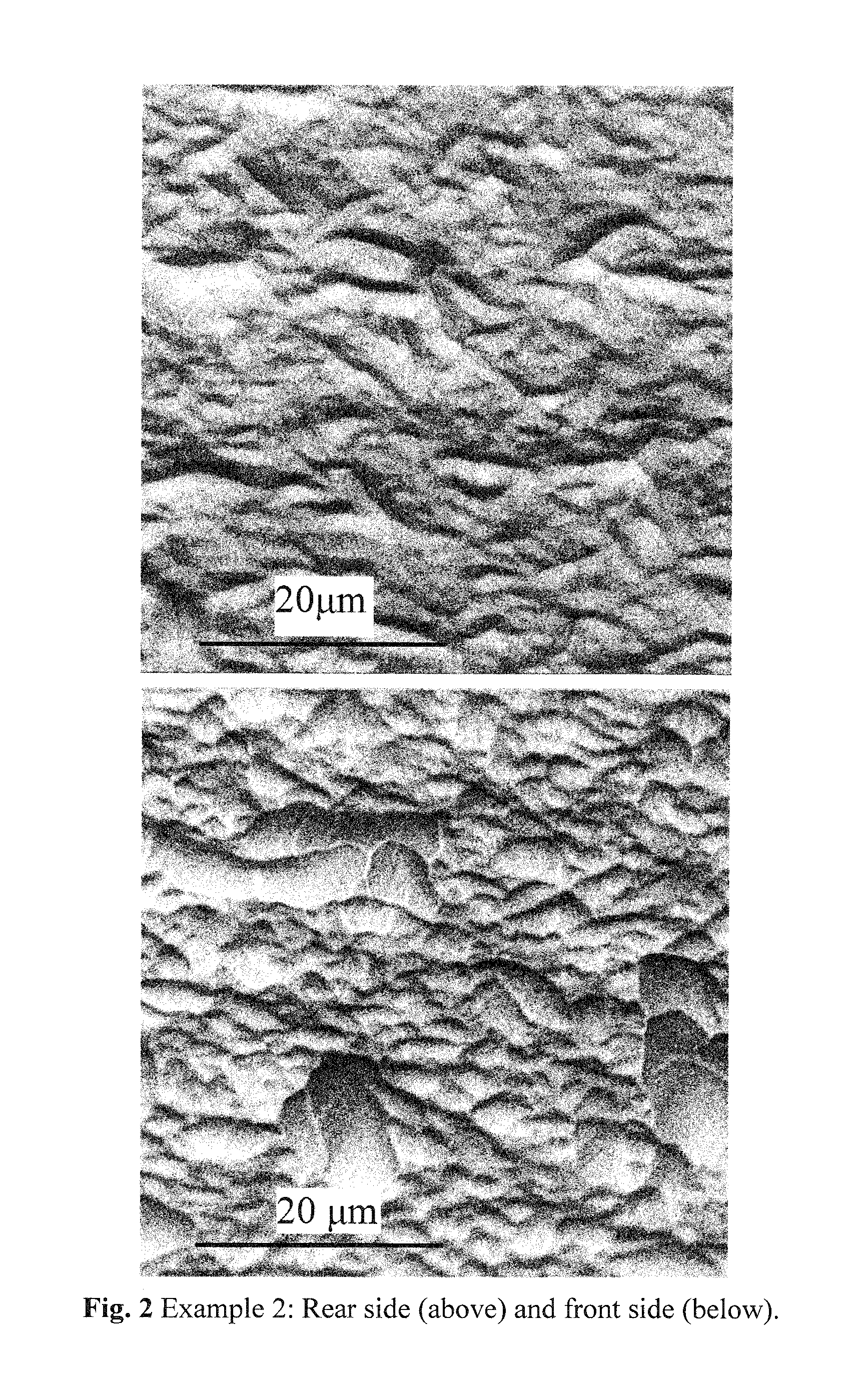
[0050]The rear side of monocrystalline Si wafer as cut were contacted with a mixture of HNO3 (67.5 wt.-% in water) and HF (49 wt.-% in water) for 3 minutes at 15 ° C. The volume ratio of HNO3 HF was 6.5:1 and a Si removal of 9.5 μm was obtained. FIG. 2 shows a SEM image of a rear side of a monocrystalline Si wafer treated with said mixture under the above conditions.

example 3

[0051]The rear side of a monocrystalline Si wafer as cut were contacted for 3 minutes at 12° C. with a mixture of HNO3 (69.5 wt.-% in water) and HF (49 wt.-% in water). The volume ratio of HNO3:HF was 9:1 and a Si removal of 7 μm was obtained. FIG. 3 shows a SEM image of a rear side of a monocrystalline Si wafer treated with said mixture under the above conditions.


PUM


Abstract

The present invention relates to a method for acidic surface etching of a silicon wafer, such as those used for solar cells, comprising contacting at least one surface of a silicon wafer as cut with an acidic etching agent, provided that the wafer is, prior to the acidic etching, not subjected to an alkaline etching step or process. Further, the present invention is directed to Si wafer, photovoltaic cells, PERC photovoltaic cells and solar modules produced according to the method of the present invention.

Description

FIELD OF THE INVENTION[0001]The present invention relates to a method for acidic surface etching of a silicon wafer, such as those used for solar cells, comprising contacting at least one surface of a pre-cleaned silicon wafer with an acidic etching agent. Further, the present invention is directed to a silicon wafer produced according to the method of the present invention and solar modules containing the same.BACKGROUND OF THE INVENTION[0002]Cut Si wafers are contaminated by metal, e.g. copper and iron. Slurry cut wafers usually contain a higher metal contamination than diamond wire sawed wafers. In a first cleaning step (Pre-Clean) the wafers have to be released from epoxy-strips (glue) that also takes away the main part of the slurry from the wafer surface together with parts of the metallic contaminants. Dependent from the glue type this cleaning process runs with hot water in combination with surfactant or without surfactant supported by ultrasonic. Common is also the usage of...

Claims


Application Information

Patent Timeline
Patent Type & Authority Applications(United States)
IPC IPC(8): H01L21/02H01L31/028
CPCH01L31/028H01L21/02019H01L31/068H01L31/1804H01L31/1868Y02E10/547Y02P70/50
Inventor HOLDERMANN, KONSTANTIN
Owner SOLARWORLD AMERICAS
Why Eureka
Try Eureka