Sers-sensor with nanostructured surface and methods of making and using

Active Publication Date: 2015-02-12
WOSTEC
View PDF0 Cites 12 Cited by
  • Summary
  • Abstract
  • Description
  • Claims
  • Application Information

AI Technical Summary

Benefits of technology

This patent describes a new surface enhanced Raman scattering (SERS) sensor that uses a nanostructured surface with elongated ridges that have a wave-ordered structure pattern. The ridges have a wavelike cross-section and are oriented perpendicular to the surface. The sensor also includes metal elements on top of the ridges to enhance the Raman signal. The method for creating the nanostructured surface involves irradiating the surface with nitrogen ions in two different directions to form a primary and secondary nanomask, which is then used to create the nanostructured surface. The wave-ordered structure pattern is created by sequential ion irradiation along two different planes of incidence separated by an azimuthal angle in a range of 30 to 90 degrees. This new sensor design has improved sensitivity and accuracy with the ability to detect single molecules.

Problems solved by technology

Disadvantages of the NSL method can include low throughput and difficulties in forming large area substrates.
Disadvantages of conventional SERS-sensors can include a low surface density of the nanospheres and metal triangles in the arrays and small array sizes which may not surpass a few millimeters.
Disadvantages of methods of manufacturing SERS-sensors based on AAO templates can include low throughput, difficulties in forming AAO templates of large area, and instability of the process of forming AAO templates induced by small deviations of critical parameters.
A disadvantage of the conventional SERS-sensor can include a small size of the AAO template which may not surpass a few centimeters.

Method used


Image

  • Sers-sensor with nanostructured surface and methods of making and using
  • Sers-sensor with nanostructured surface and methods of making and using
  • Sers-sensor with nanostructured surface and methods of making and using

Examples


Embodiment Construction

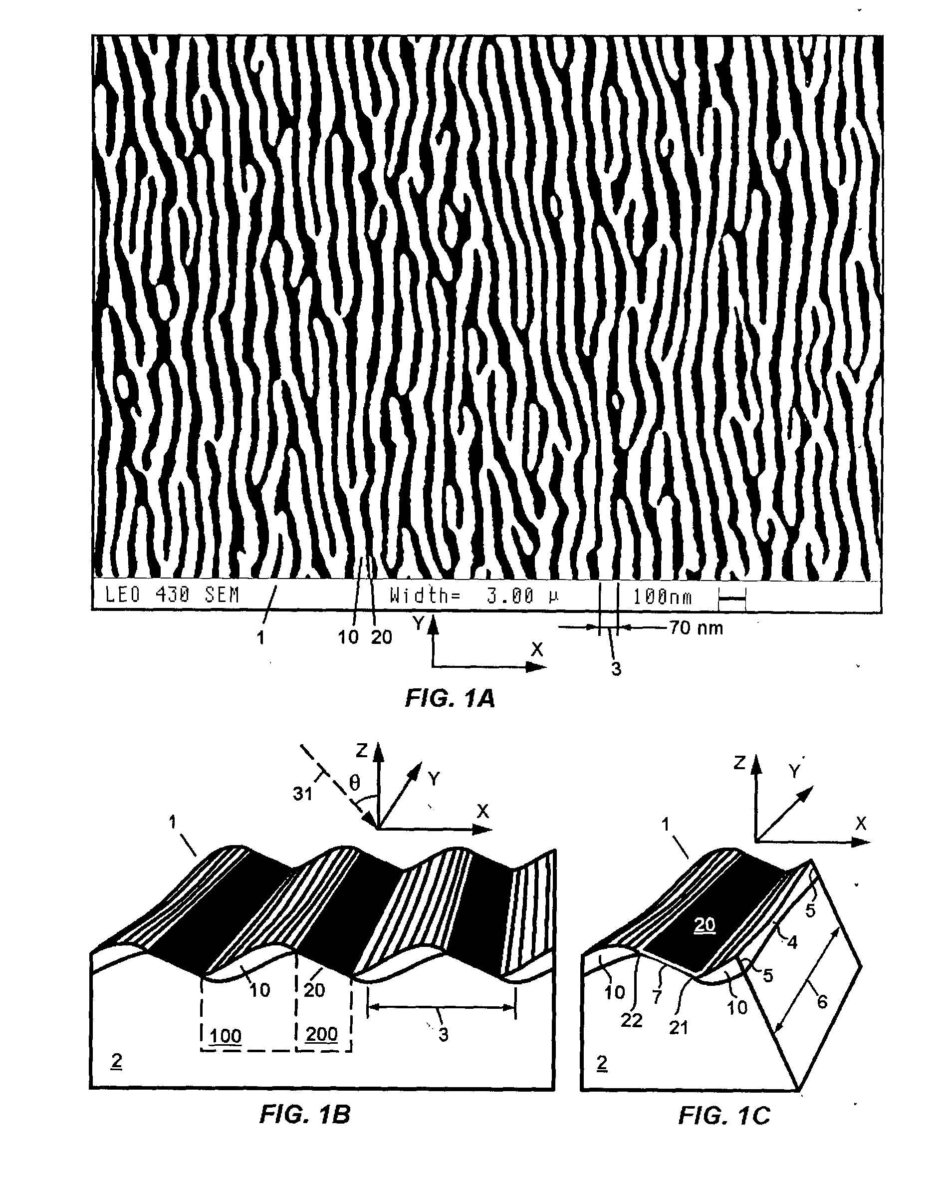
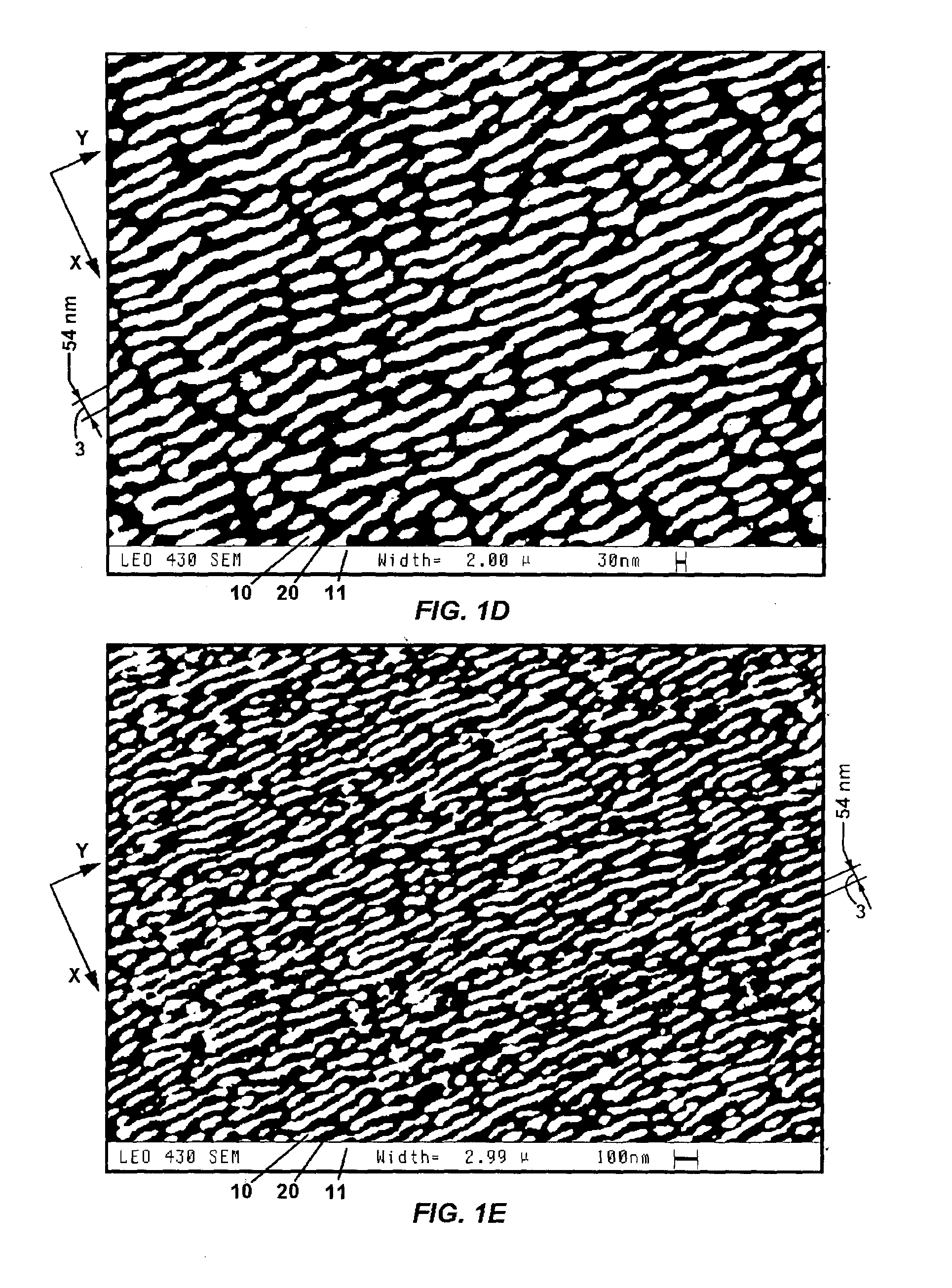
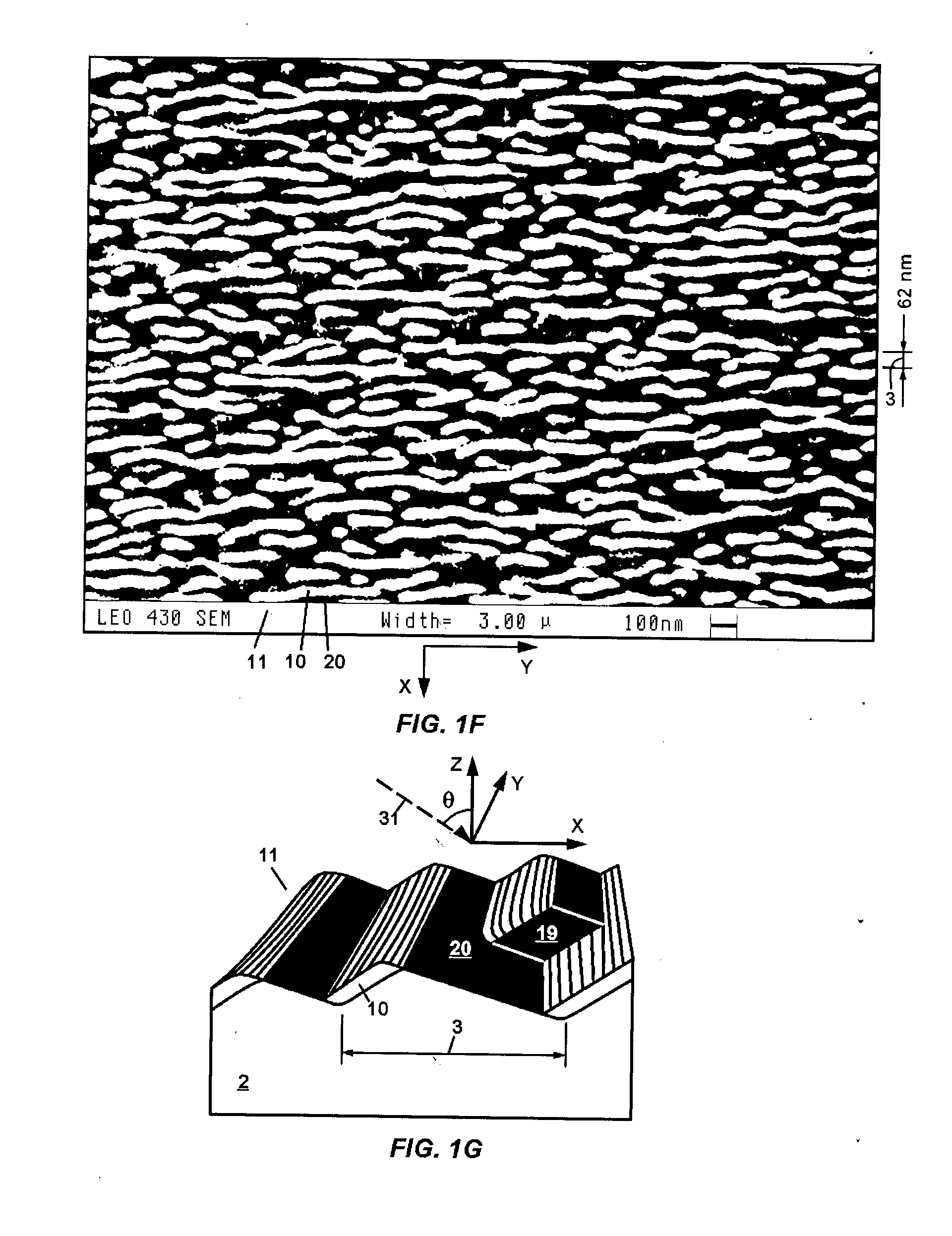
[0041]The invention relates to the field of optical sensors for detecting and measuring the traces of organic compounds by the method of Raman spectroscopy using the effect of surface enhanced Raman scattering (SERS). The invention also relates to the technology of forming nanostructured elements on the surface of substrates for optical sensors (SERS-sensors) for measuring Raman scattering signal from analyte molecules positioned on the nanostructured surface of the sensor.

[0042]For example, a SERS-sensor includes a substrate with a nanostructured surface. The nanostructured surface includes an array of ridge elements, which may be formed using a wavelike silicon nitride nanomask. This nanomask is self-formed during the irradiation of the silicon substrate surface by a beam of nitrogen ions. The nanomask is also self-formed during the irradiation of a silicon layer on the substrate surface by a beam of nitrogen ions. As a result of etching of the substrate through the nanomask a den...


PUM


Abstract

A surface enhanced Raman scattering (SERS) sensor includes a substrate with a nanostructured surface. The nanostructured surface has a quasi-periodic, anisotropic array of elongated ridge elements having a wave-ordered structure pattern, each ridge element having a wavelike cross-section and oriented substantially in a first direction. The sensor also includes a plurality of metal elements disposed, at least in part, on tops of the ridge elements.

Description

FIELD[0001]The invention relates to the field of optical sensors for detecting and measuring the traces of organic compounds by the method of Raman spectroscopy using the effect of surface enhanced Raman scattering (SERS). The invention also relates to the technology of forming nanostructured elements on the surface of substrates for optical sensors (SERS-sensors) for measuring Raman scattering signal from analyte molecules positioned on the nanostructured surface of the sensor.BACKGROUND[0002]There is a general interest in the manufacture and use of optical sensors (SERS-sensors) with nanostructured metal surface. FIG. 16A illustrates one type of conventional SERS-sensor with nanostructured metal coverage. This SERS-sensor includes a substrate 161 of copper or silicon oxide, a dense hexagonal array of nanospheres 162 of polystyrene or silicon oxide arranged on the substrate surface, and a metal film 28 over the array of nanospheres (U.S. Patent Application Publication No. 2009 / 0118...

Claims


Application Information

Patent Timeline
IPC IPC(8): G01N21/65
CPCG01N2201/06113G01N21/65B81C1/00031G01N21/658Y10T428/24479
Inventor SMIRNOV, VALERY K.KIBALOV, DMITRY S.
Owner WOSTEC
Why Eureka
Try Eureka