Method for manufacturing multi-layered printed circuit board

Inactive Publication Date: 2015-03-05
SAMSUNG ELECTRO MECHANICS CO LTD
View PDF17 Cites 2 Cited by
  • Summary
  • Abstract
  • Description
  • Claims
  • Application Information

AI Technical Summary

Benefits of technology

The present invention provides a method for forming holes in a copper foil surface using a laser process without causing damage or degradation to the resin. The surface is treated to increase absorption of the laser and provide an anchor effect for better adhesion of copper plating. The resulting copper foil is a composite foil with high laser absorption, excellent adhesion, heat resistance, and chemical resistance, which provides a method for treating the surface of copper foil.

Problems solved by technology

It is very difficult to form a hole having a diameter of about 200 μm or less using a mechanical drill.
The reason is that process speed is relatively slow, process accuracy is low, product characteristics is likely to be changed due to thermal diffusion, and defect is caused by abrasion of drill bits.
There were many attempts to machine a copper foil with the laser, but it was difficult to form the hole in a thick copper foil since the copper foil has low laser absorption coefficient and an outer layer of the copper foil reflects the laser.
However, this manufacturing method degrades production efficiency due to the increased etching processes.
In this case, there was a disadvantage in that adhesion strength between the outer layer formed with the copper plating and the insulation layer became low.
This proposes a method in which the copper foil for processing the hole is formed to be thin and the copper foil is bored at a time by using laser having high energy, but does not disclose a specific example about a method for controlling reflection.
Therefore, this method has low generality.

Method used


Image

  • Method for manufacturing multi-layered printed circuit board
  • Method for manufacturing multi-layered printed circuit board
  • Method for manufacturing multi-layered printed circuit board

Examples


first preferred embodiment

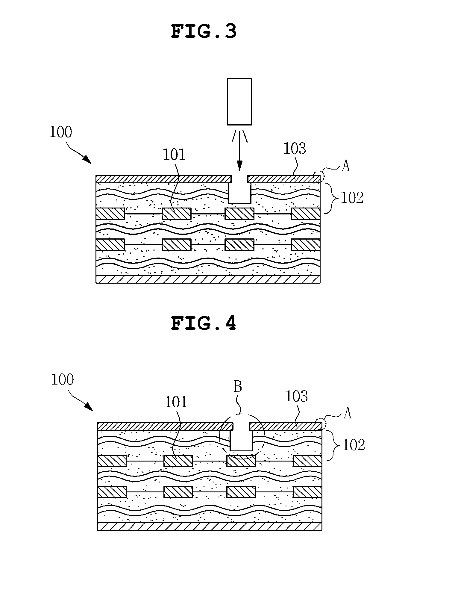
[0053]FIGS. 1 to 8 are process flow charts schematically showing a method for manufacturing a multi-layered printed circuit board according to a preferred embodiment of the present invention and processes of forming a through-hole 201 by a two-step processing may be confirmed therefrom.

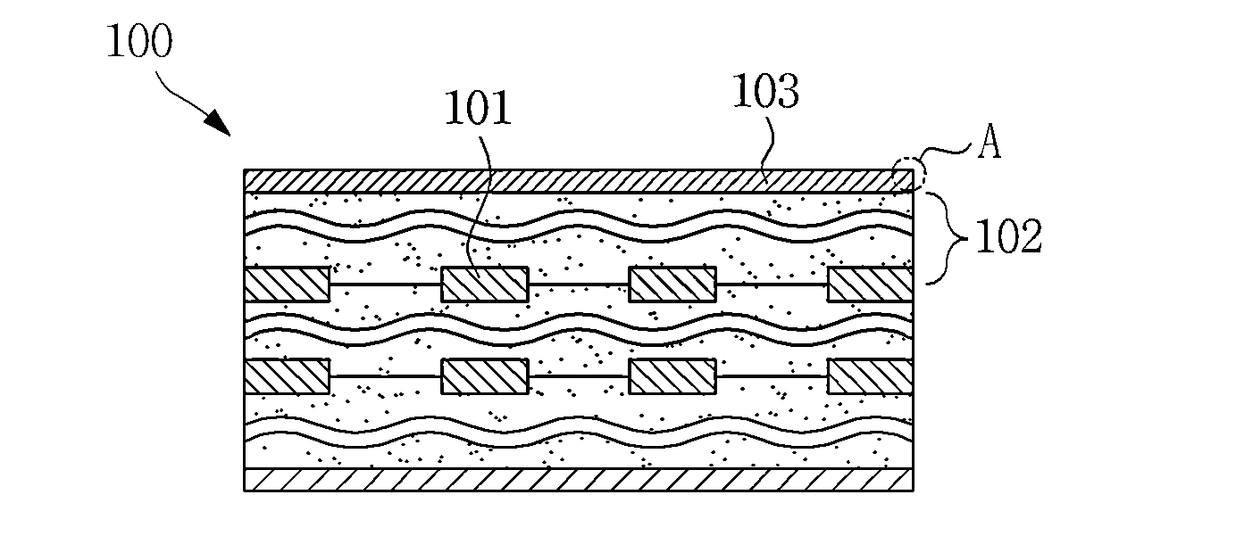
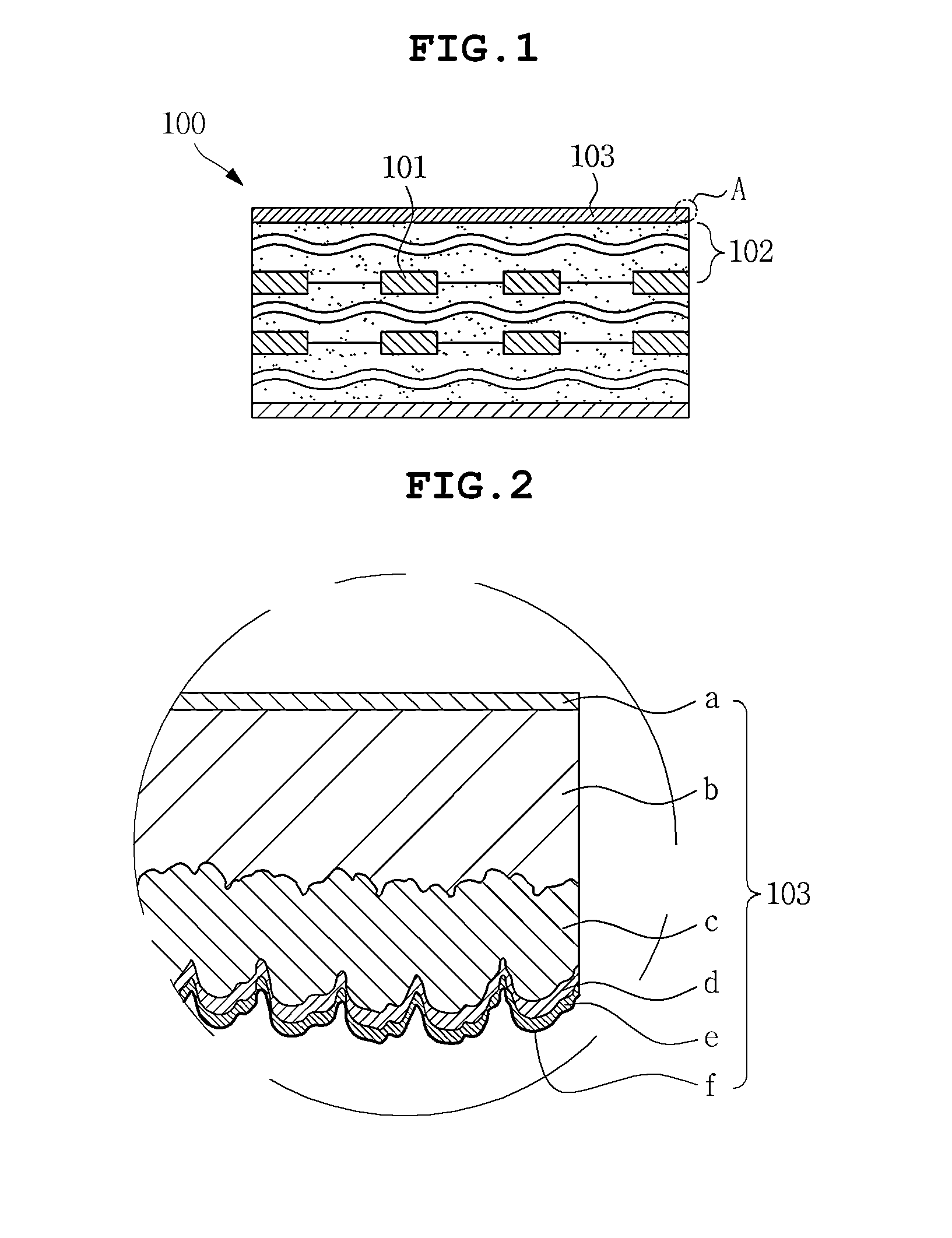
[0054]According to the preferred embodiment of the present invention, the method for manufacturing the multi-layered printed circuit board may include an operation of preparing a substrate 100 having an insulating layer 102 and a surface-treated copper foil 103 sequentially formed on an inner layer circuit 101, an operation of forming a hole 200 exposing the insulating layer 102 by performing a primary processing for the surface-treated copper foil 103 and a part of the insulating layer 102 with laser, and an operation of forming a through hole 201 exposing the inner layer circuit 101 by performing a secondary processing for the exposed insulating layer 102 with a chemical etching liquid.

[0055]Referri...

second preferred embodiment

[0087]FIGS. 9 to 15 are process flow charts schematically showing a method for manufacturing a printed circuit board according to another preferred embodiment of the present invention and processes of forming a radiation hole 401 by two-step processing may be confirmed therefrom.

[0088]According to another preferred embodiment of the present invention, the method for manufacturing the printed circuit board may include an operation of preparing a substrate 300 having an insulating layer 302 and a surface-treated copper foil 303 sequentially formed on an inner layer circuit 301, an operation of forming a hole 400 by performing a primary processing for the surface-treated copper foil 303 and a part of the insulating layer 302 with laser, and an operation of forming a radiation hole 401 performing a secondary processing for the insulating layer 302 in the primarily processed hole 400 with a chemical etching liquid and removing another part of the partially removed insulating layer 302 to...


PUM

PropertyMeasurementUnit
Lengthaaaaaaaaaa
Lengthaaaaaaaaaa

Abstract

Disclosed herein is a method for manufacturing a multi-layered printed circuit board, the method including: an operation of preparing a substrate having an insulating layer and a surface-treated copper foil sequentially formed on an inner layer circuit; an operation of forming a hole exposing the insulating layer by performing a primary processing for the surface-treated copper foil and a part of the insulating layer with laser; and an operation of forming a through-hole exposing the inner layer circuit by performing a secondary processing for the exposed insulating layer with a chemical etching liquid.

Description

CROSS REFERENCE TO RELATED APPLICATION[0001]This application claims the benefit of Korean Patent Application No. 10-2013-0101932, filed on Aug. 27, 2013, entitled “Method for Manufacturing Multi-Layered Printed Circuit Board”, which is hereby incorporated by reference in its entirety into this application.BACKGROUND OF THE INVENTION[0002]1. Technical Field[0003]The present invention relates to a method for manufacturing a multi-layered printed circuit board.[0004]2. Description of the Related Art[0005]In accordance with miniaturization, lightness, and high-performance of an electronic device, reduction in a circuit width and a small-caliber of a via hole connecting layers to each other have been demanded.[0006]It is very difficult to form a hole having a diameter of about 200 μm or less using a mechanical drill. The reason is that process speed is relatively slow, process accuracy is low, product characteristics is likely to be changed due to thermal diffusion, and defect is caused ...

Claims


Application Information

Patent Timeline
IPC IPC(8): H05K3/46
CPCH05K3/4685H05K2203/0353H05K3/4644H05K3/002H05K3/0038H05K3/429H05K2203/0307H05K2203/0392H05K2203/107Y10T29/49165H05K3/46
Inventor HAN, YOUN GYULEE, DONG KYOUNG
Owner SAMSUNG ELECTRO MECHANICS CO LTD
Why Eureka
Try Eureka