

Semiconductor component
a technology of semiconductors and components, applied in the field of semiconductor components, can solve the problems of inability to obtain a high on/off ratio, complex production of previously designed components, and electrodes no longer contributing to the conductivity, and achieve the effect of simple production
- Summary
- Abstract
- Description
- Claims
- Application Information
AI Technical Summary
Benefits of technology
Problems solved by technology
Method used
Image

Examples
first embodiment
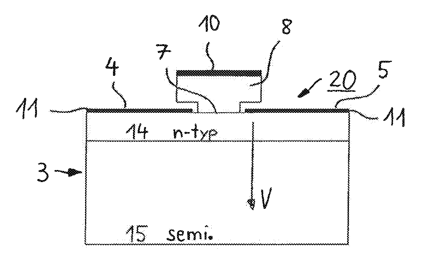
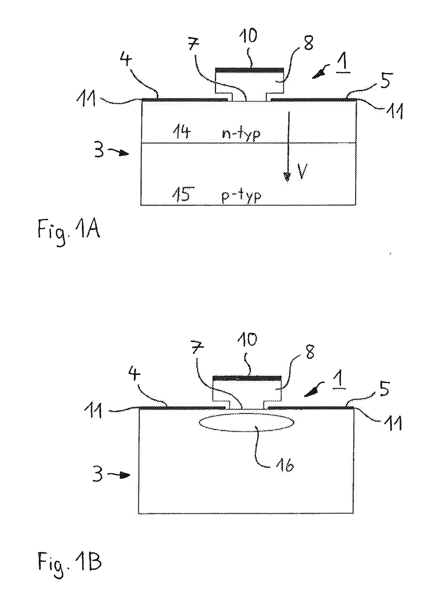
[0045]FIG. 1A schematically illustrates a cross section of a semiconductor component 1 in accordance with a first embodiment variant. The semiconductor component 1 comprises a semiconductor substrate 3 composed of silicon carbide, to the surface of which a source electrode 4 and a drain electrode 5 separate therefrom are applied. In an exposed intermediate region 7 of the semiconductor substrate 3 between the source electrode 4 and the drain electrode 5, a gate stack is formed by a dielectric 8, on the top side of which a gate electrode 10 is arranged.
[0046]The source electrode 4 and the drain electrode 5 comprise at least one monolayer of epitaxial graphene 11 grown on a surface of the silicon carbide crystal. By way of example, the surface of the silicon carbide is a (0001) surface. The at least one monolayer of epitaxial graphene 11 is produced on the surface of the silicon carbide by thermal decomposition of the silicon carbide. The two electrodes 4, 5 are subsequently produced ...
second embodiment
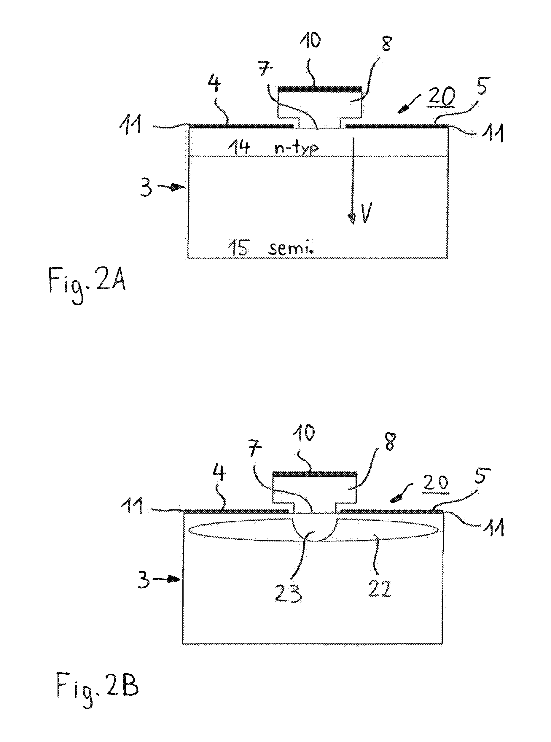
[0053]FIG. 2A illustrates a semiconductor component 20 in accordance with a second embodiment variant in a cross section. In this case, identical reference signs designate identical parts.
[0054]In a manner corresponding to FIG. 1A, the semiconductor component 20 in accordance with FIG. 2A also comprises a semiconductor substrate 3 composed of silicon carbide, to the surface of which a source electrode 4 and a drain electrode 5 are applied, which comprise at least one monolayer of epitaxial graphene 11 on the silicon carbide surface. The electrodes 4, 5 of the semiconductor component 20 according to FIG. 2A are likewise produced by means of thermal decomposition of the surface of the silicon carbide.
[0055]A gate stack comprising a dielectric 8 and a gate electrode 10 applied thereto is once again arranged in an intermediate region 7 between the source electrode 4 and the drain electrode 5.
[0056]Like FIG. 1A, the semiconductor substrate 3 of the semiconductor component 20 according to...
third embodiment
[0059]FIG. 3 illustrates a semiconductor component 30 in accordance with a third embodiment variant in a plan view and in a cross section. In this case, identical parts are once again provided with identical reference signs.
[0060]In the case of the semiconductor component 30 in accordance with FIG. 3, the semiconductor substrate 3 likewise has a vertical n-p junction beneath the electrodes 4, 5. A space charge zone SCZ arises which extends far into the first, n-conducting region 14 of the silicon carbide. The doping concentrations and the vertical thicknesses of the regions 14, 15 can vary relative to the semiconductor component 1 illustrated in FIG. 1.
[0061]In contrast to the semiconductor component 1 illustrated in FIG. 1, no dielectric 8 is applied in the intermediate region 7 between the source electrode 4 and the drain electrode 5. Rather, an electrochemical electrode is used as a gate electrode 10. For this purpose, a drop of an ionic liquid 31 is applied between the two elect...
PUM
 Abstract
Description
Claims
Application Information