Method and Apparatus for Limiting Startup Inrush Current for Low Dropout Regulator
a technology of inrush current and startup current, which is applied in the direction of electric variable regulation, process and machine control, instruments, etc., can solve the problems of large inrush current and unsuitable large inrush current, and achieve the effect of low dropou
- Summary
- Abstract
- Description
- Claims
- Application Information
AI Technical Summary
Benefits of technology
Problems solved by technology
Method used
Image
Examples
second embodiment
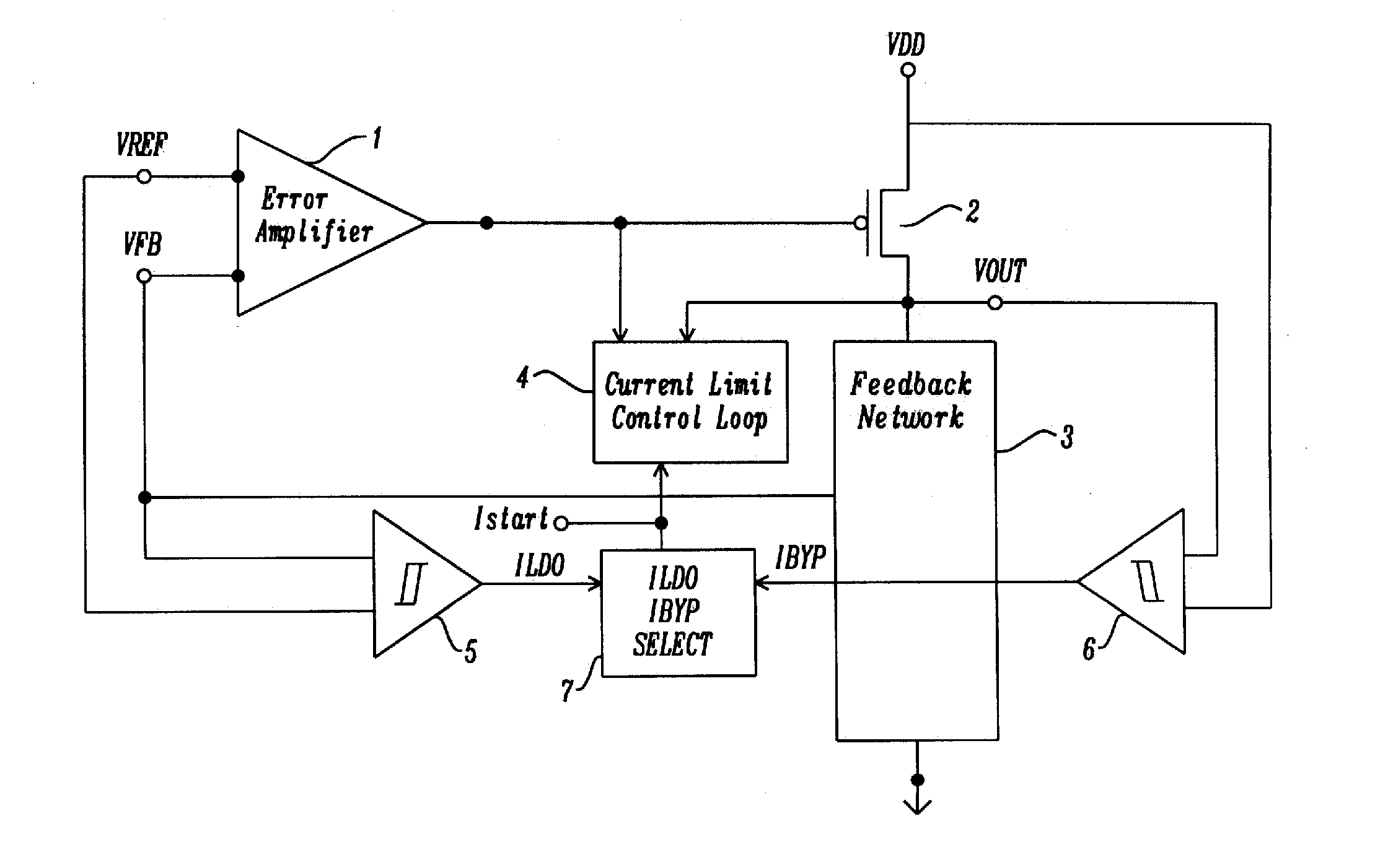
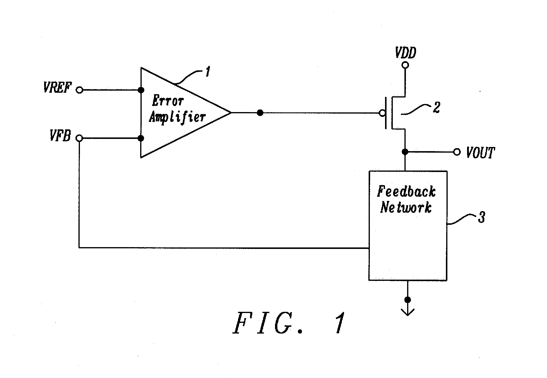
[0046]FIG. 5 a circuit schematic diagram illustrating a low dropout (LDO) regulator with current limit control loop and comparators in accordance with the disclosure. An LDO regulator consists of an error amplifier 1, pass transistor 2, and a feedback network 3, and a current limit control loop 4, a VREF / VFB LDO mode comparator 5, a VOUT / VDD Bypass mode comparator 6, and a ILDO / IBYP select control 7. The pass transistor 2 is a p-channel metal oxide semiconductor field effect transistor (MOSFET). The pass transistor 2 has a MOSFET source connected to voltage VDD, and whose p-channel MOSFET drain connected to output voltage, VOUT, and whose MOSFET gate is connected to the output of error amplifier 1. The error amplifier 1 has a negative input defined as voltage reference input, VREF, and a second positive input signal feedback voltage, VFB. The feedback network 3 is connected between the p-channel MOSFET output voltage VOUT, and ground reference VSS. The feedback network 3 can consist...
third embodiment
[0052]FIG. 10 is a circuit schematic diagram illustrating a low dropout (LDO) regulator for modifying the sensed current at startup with a series cascode p-channel pull-up in accordance with the disclosure. The circuit contains a current source 12 between the VDD signal and control signal ICTRL. A current mirror network is formed with n-channel MOSFET N1, and n-channel MOSFET N2. Current control 11 is coupled to the n-channel current mirror network formed with n-channel MOSFET N1, and n-channel MOSFET N2. A second current mirror network is formed with p-channel MOSFET P1, and p-channel MOSFET P2. The second current mirror network is coupled to output voltage VOUT, and current source 10. A switch S1 is placed in series with p-channel MOSFET P3. P-channel MOSFET P3 is in series with a p-channel MOSFET P4. The gate voltage, VGATE, is connected to both the gate connection to p-channel MOSFET P3, and p-channel MOSFET P4. The sensed current is increased in startup to reduce the current li...
fourth embodiment
[0053]FIG. 11 is a circuit schematic diagram illustrating a low dropout (LDO) regulator for modifying the sensed current at startup with parallel p-channel pull-up in accordance with the disclosure. The circuit contains a current source 12 between the VDD signal and control signal ICTRL. A current mirror network is formed with n-channel MOSFET N1, and n-channel MOSFET N2. Current control 11 is coupled to the n-channel current mirror network formed with n-channel MOSFET N1, and n-channel MOSFET N2. A second current mirror network is formed with p-channel MOSFET P1, and p-channel MOSFET P2. The second current mirror network is coupled to output voltage VOUT, and current source 10. A switch S1 is placed in series with p-channel MOSFET P6. P-channel MOSFET P5 is in parallel with a p-channel MOSFET P6. The gate voltage, VGATE, is connected to both the gate connection to p-channel MOSFET P5 AND p-channel MOSFET P6. The sensed current is increased in startup to reduce the current limit. At...
PUM
 Abstract
Description
Claims
Application Information


