
Eureka
For R&D, Eureka makes reading and utilizing patents & technical documents easy.
Eureka AIR
Designed for self-driven R&D workflows. Generate viable solutions, solve complex R&D challenges, empower your innovation with AI.

Eureka Materials
Designed for material experts only. Revolutionize your material R&D, from search, analyze, to developing new materials.

TechResearch
Generate reliable direction feasibility study reports for your R&D in just a few steps.

TechSeek
Discover and master advanced knowledge NOW. Basics, ideas, possibilities, all at once.

TechMind
As an expert in R&D Theories, TechMind can generates customized viable solutions instantly.

TechRisk
Analyze your overall solution with one click, know your potential R&D risks in advance.

TechMonitor
Get weekly tech updates, stay abreast of the latest tech innovations and key insights.
Imaging device, method of driving imaging device, and camera
- Summary
- Abstract
- Description
- Claims
- Application Information
AI Technical Summary
Benefits of technology
Problems solved by technology
Method used
Image

Examples
embodiment 1
Configuration of Image Sensor
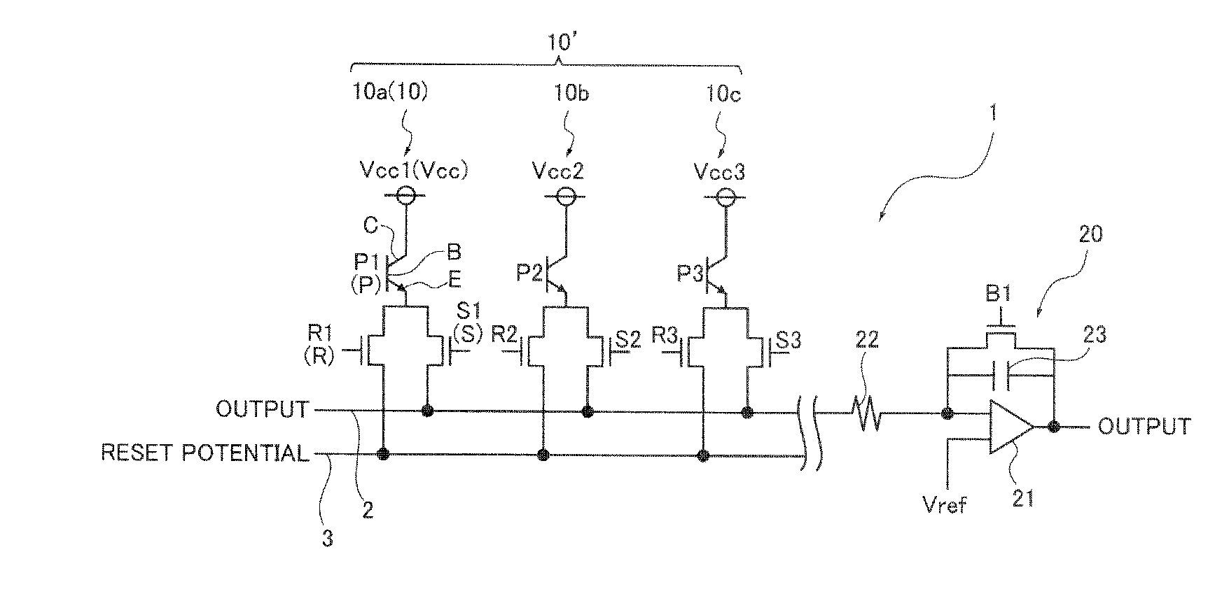
[0024]Hereinafter, one embodiment of the imaging device according to the present invention will be described with reference to the drawings. FIG. 1 is an equivalent circuit schematic of an image sensor 1 as an imaging device according to Embodiment 1 of the present invention. As illustrated in FIG. 1, the image sensor 1 according to Embodiment 1 includes a pixel array 10′ having a plurality of pixels 10 (10a, 10b, 10c) arranged in an array, an integration amplifier 20 provided in the pixel array 10′, an output line 2 as a signal charge readout path, and a reset line 3 as an alternative path provided separately from the output line 2. Only one pair (one line) of the pixel array 10′ and the integration amplifier 20 is illustrated in FIG. 1. However, in Embodiment 1, plural pairs (plural lines) of the pixel array 10′ and the integration amplifier 20 are disposed. The image sensor 1 in which the pixels 10 are two-dimensionally arranged in a matrix is thereby...
embodiment 2
[0056]Next, in Embodiment 2, one example of a camera including the imaging device of the present invention (for example, digital still camera or digital video camera) will be described with reference to FIG. 7. FIG. 7 is a block diagram illustrating the system configuration of a camera 100 of Embodiment 2. As illustrated in FIG. 7, the camera 100 of Embodiment 2 includes a photographing lens 110 as an imaging optical system, an image sensor 120 as an imaging element (imaging device of present invention), a signal processor 130, an operation unit 140, a controller (CPU) 150, a liquid crystal monitor (LCD) 160 as a display, a driver 170, and a memory card 180. The camera 100 includes a monitoring camera which is fixed in an outside, and continuously photographs a moving picture in addition to a digital camera and a video camera which photograph a still image and a moving picture.
[0057]The imaging lens 110 as the imaging optical system includes a plurality of lens groups such as a zoom...
PUM
 Abstract
Description
Claims
Application Information
 - R&D Engineer
- R&D Manager
- IP Professional
- Industry Leading Data Capabilities
- Powerful AI technology
- Patent DNA Extraction
Browse by: Latest US Patents, China's latest patents, Technical Efficacy Thesaurus, Application Domain, Technology Topic, Popular Technical Reports.
© 2024 PatSnap. All rights reserved.Legal|Privacy policy|Modern Slavery Act Transparency Statement|Sitemap|About US| Contact US: help@patsnap.com