Method for manufacturing semiconductor device

Inactive Publication Date: 2015-03-19
SEMICON ENERGY LAB CO LTD
View PDF5 Cites 17 Cited by
  • Summary
  • Abstract
  • Description
  • Claims
  • Application Information

AI Technical Summary

Benefits of technology

The present invention provides an oxide semiconductor layer with fewer defects and improved reliability for transistors including oxide semiconductor. Additionally, the invention improves the electrical characteristics of semiconductor devices including oxide semiconductor. The method involves forming an oxide semiconductor layer without plasma damage and with high crystallinity. This results in a channel of a transistor that has improved reliability and performance. The invention has wide-ranging applications and is not limited to the effects described.

Problems solved by technology

In a transistor including an oxide semiconductor, a defect in an oxide semiconductor layer or a bond of the defect with hydrogen or the like might cause a carrier in a film, which might change the electrical characteristics of the transistor.

Method used


Image

  • Method for manufacturing semiconductor device
  • Method for manufacturing semiconductor device
  • Method for manufacturing semiconductor device

Examples


embodiment 1

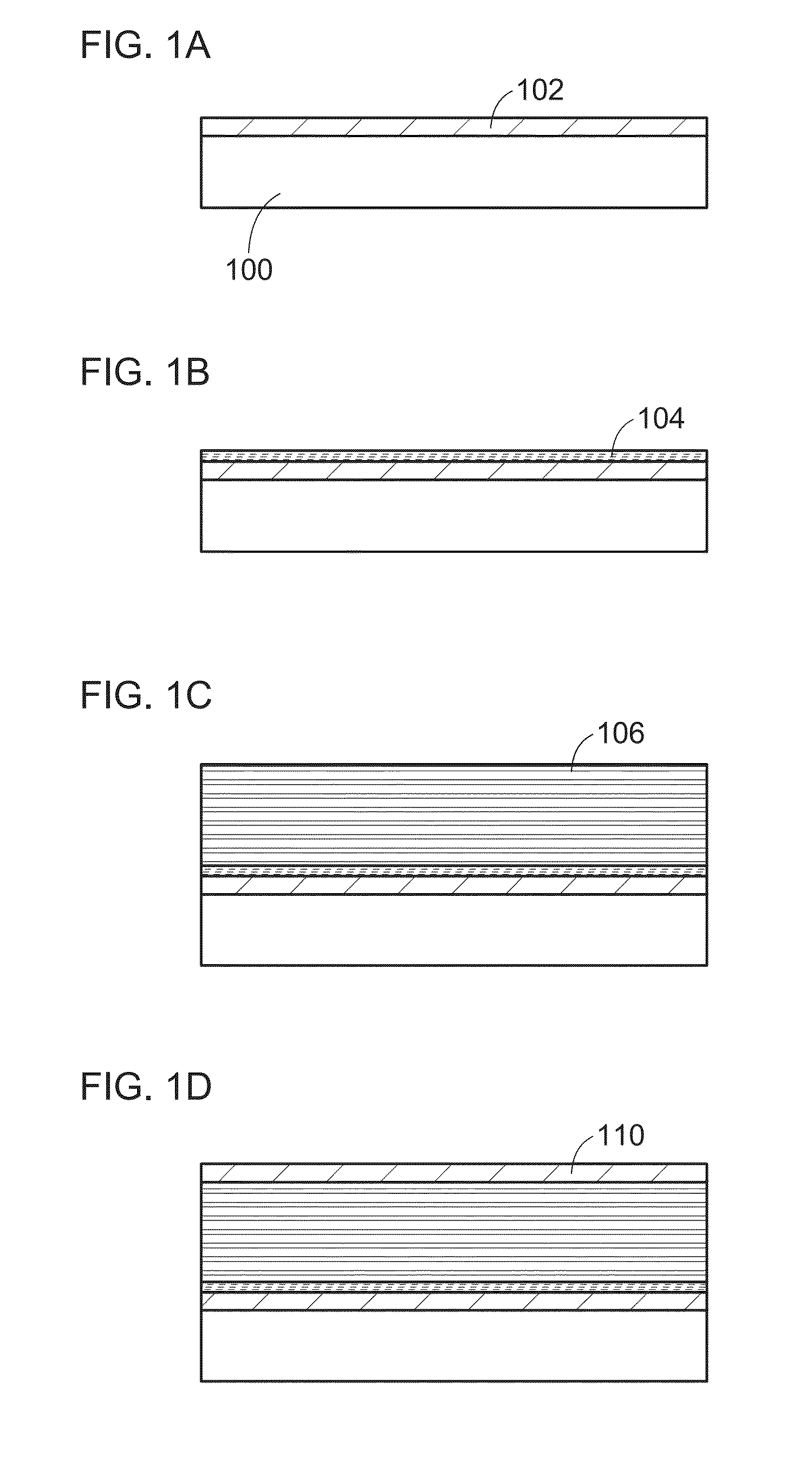
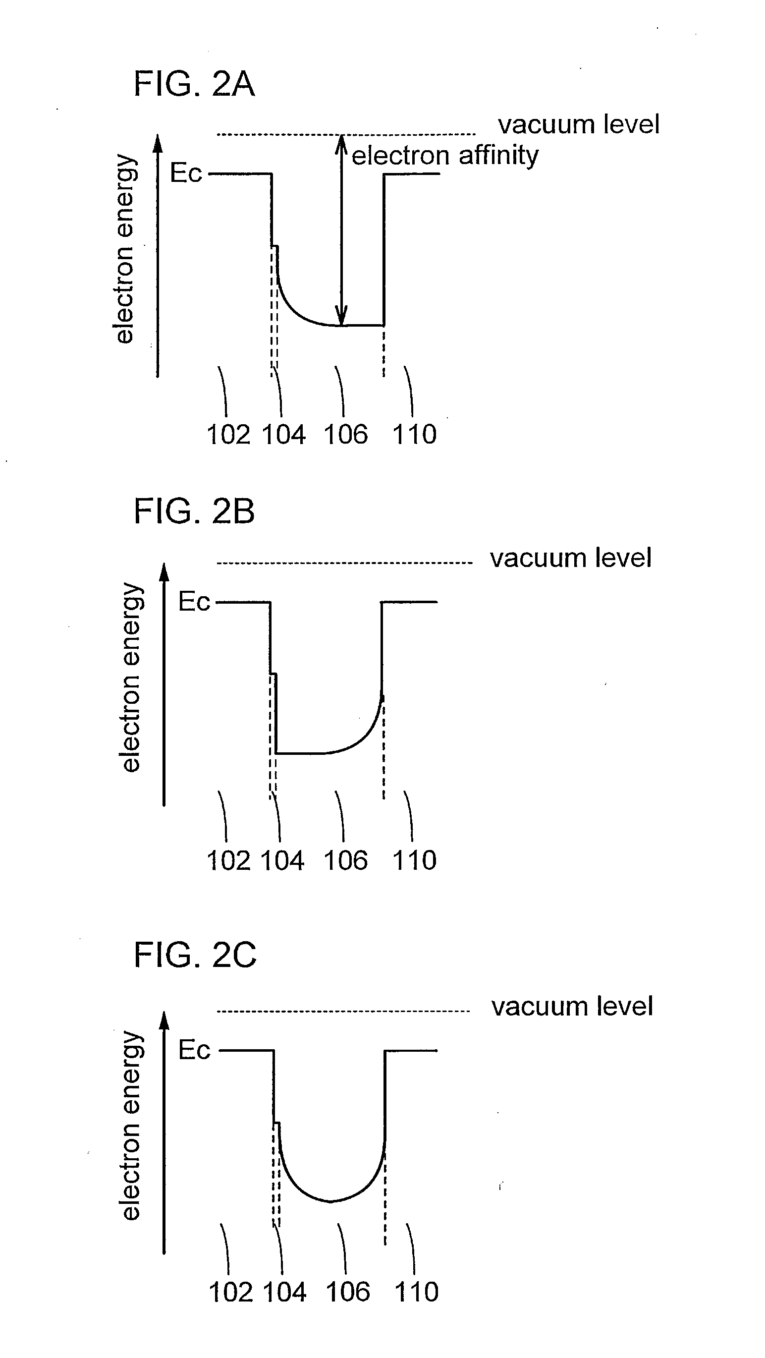
[0056]In this embodiment, a method of forming an oxide semiconductor layer that can be used in a semiconductor device of one embodiment of the present invention will be described with reference to drawings.

[0057]In one embodiment of the present invention, a first oxide semiconductor layer is formed over a substrate by a sputtering method, and a second oxide semiconductor layer is formed by epitaxial growth using the first oxide semiconductor layer as a seed crystal. Here, a thermal chemical vapor deposition (thermal CVD) method is employed for the formation of the second oxide semiconductor layer. The thermal CVD method is different from a plasma CVD method by which a source gas of a main component of a film is decomposed by plasma. By the thermal CVD method, a source gas is decomposed by heating over a heated substrate; thus, in the second oxide semiconductor layer formed by the thermal CVD method, plasma damage is prevented and the number of defects is reduced. For example, in the...

embodiment 2

[0122]In this embodiment, described will be specific examples of a manufacturing apparatus with which an oxide semiconductor layer and the like of one embodiment of the present invention can be formed.

[0123]A manufacturing apparatus illustrated in FIG. 3A includes at least a load chamber 302, a transfer chamber 310, a pretreatment chamber 303, a treatment chamber 304 which is a deposition chamber using a sputtering method, a treatment chamber 331 which is a deposition chamber using a thermal CVD method, and an unload chamber 306. With the manufacturing apparatus illustrated in FIG. 3A, films can be formed successively without being exposed to the air. Therefore, in the case where a stacked structure is formed, an impurity can be prevented from entering a film or an interface between films. Note that in order to prevent, for example, attachment of moisture to inner walls of chambers (including a load chamber, a treatment chamber, a transfer chamber, a deposition chamber, and an unloa...

embodiment 3

[0138]In this embodiment, the structure of a transistor of one embodiment of the present invention having the stacked structure described in Embodiment 1 will be described.

[0139]FIGS. 4A and 4B are a plan view and a cross-sectional view illustrating a transistor 450 of one embodiment of the present invention. FIG. 4A is a plan view and FIG. 4B is a cross-sectional view taken along dashed-dotted line A1-A2 and dashed-dotted line A3-A4 in FIG. 4A. Note that for simplification of the drawing, some components are not illustrated in the plan view in FIG. 4A.

[0140]The transistor 450 illustrated in FIGS. 4A and 4B includes an insulating layer 402 having a projecting portion over a substrate 400; a first oxide semiconductor layer 404 and a second oxide semiconductor layer 406 over the projecting portion of the insulating layer 402; a source electrode layer 408a and a drain electrode layer 408b which are in contact with side surfaces of the first oxide semiconductor layer 404 and a top surfa...


PUM


Abstract

Provided are an oxide semiconductor layer in which the number of defects is reduced and a highly reliable semiconductor device including the oxide semiconductor. A first oxide semiconductor layer having a crystal part is formed over a substrate by a sputtering method. A second oxide semiconductor layer is formed by a thermal chemical vapor deposition method over the first oxide semiconductor layer. The second oxide semiconductor layer is formed by epitaxial growth using the first oxide semiconductor layer as a seed crystal. A channel is formed in the second oxide semiconductor layer.

Description

BACKGROUND OF THE INVENTION[0001]1. Field of the Invention[0002]The present invention relates to an object, a method, or a manufacturing method. The present invention relates to a process, a machine, manufacture, or a composition of matter. In particular, one embodiment of the present invention relates to a semiconductor device or a method of manufacturing the semiconductor device.[0003]In this specification and the like, the term “semiconductor device” means all devices that can operate by utilizing semiconductor characteristics. An electro-optical device, an image display device (also referred to as display device), a semiconductor circuit, a light-emitting device, a power storage device, a memory device, or an electronic device include a semiconductor device in some cases.[0004]2. Description of the Related Art[0005]A technique in which a transistor is formed using a semiconductor layer has attracted attention. The transistor is used in a wide range of electronic devices such as ...

Claims


Application Information

Patent Timeline
IPC IPC(8): H01L21/28H01L21/441
CPCH01L21/441H01L21/28008H01L21/02472H01L21/02483H01L21/02502H01L21/02554H01L21/02565H01L21/0262H01L21/02631H01L29/42384H01L29/66969H01L29/7869H01L29/78696
Inventor YAMAZAKI, SHUNPEI
Owner SEMICON ENERGY LAB CO LTD
Why Eureka
Try Eureka