

Resistor memory bit-cell and circuitry and method of making the same
- Summary
- Abstract
- Description
- Claims
- Application Information
AI Technical Summary
Benefits of technology
Problems solved by technology
Method used
Image

Examples
first embodiment
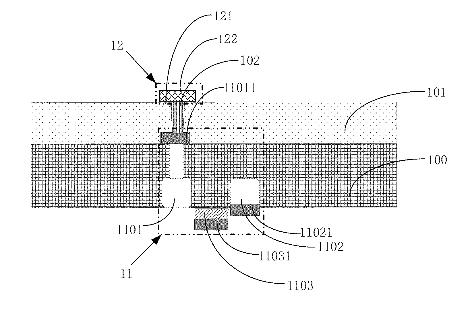
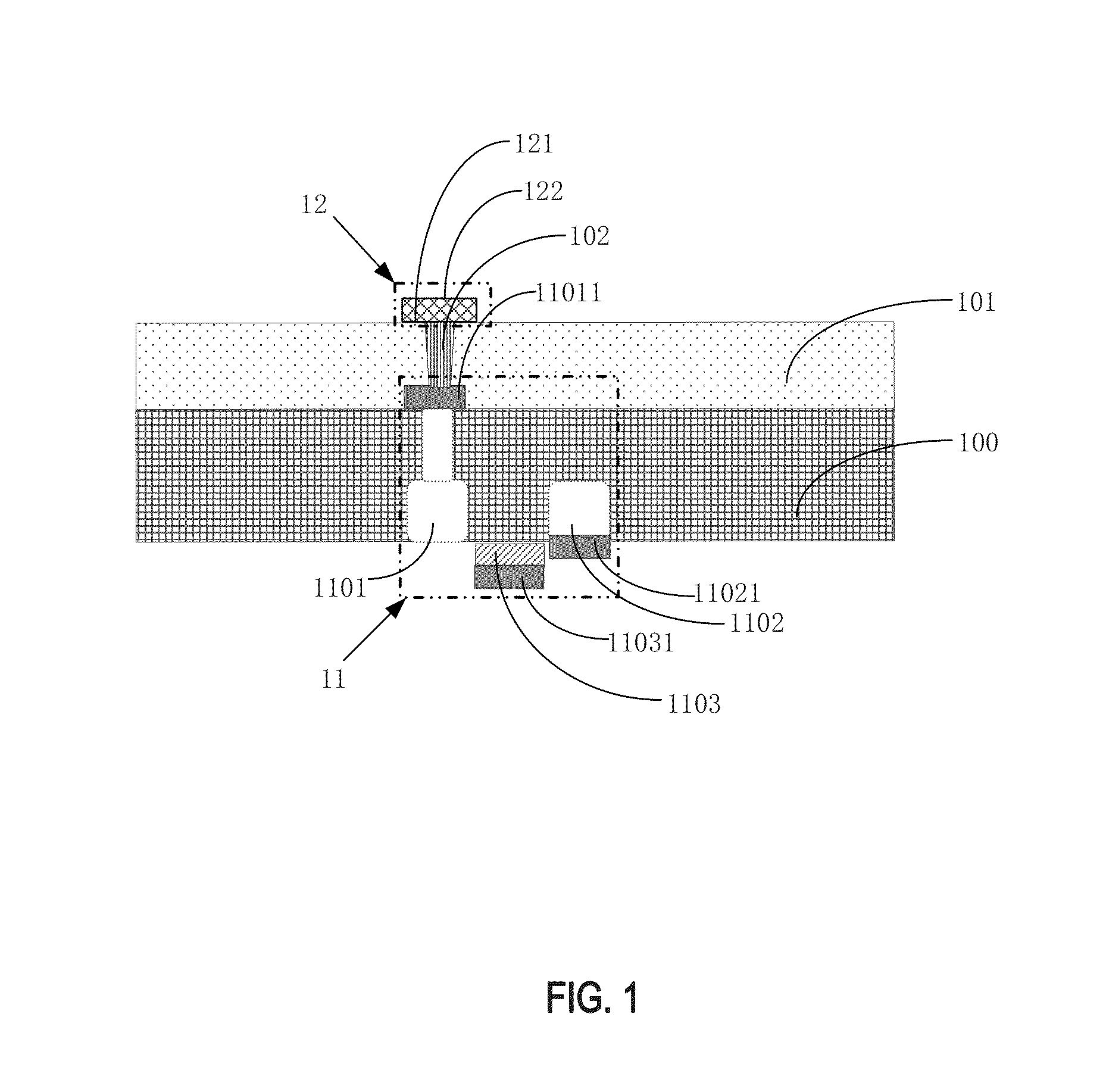
[0028]According to a first embodiment, a semiconductor memory control unit includes a switching transistor disposed on a first surface of a semiconductor substrate and a resistive memory cell disposed on an opposite second surface of the semiconductor substrate. The switching transistor includes agate electrode on the first surface (upper surface) of the semiconductor substrate, a source electrode, and a drain electrode disposed in the semiconductor substrate. The switching transistor also includes, on the first surface, a source terminal connected to the source electrode and agate terminal connected to the gate electrode. The switching transistor further includes, on the second surface (lower surface) of the semiconductor substrate, a drain terminal connected to the drain electrode. The resistive memory cell has a first end that is connected to the drain electrode through the drain terminal of the switching transistor.
[0029]The structure of the semiconductor memory control unit acc...
second embodiment
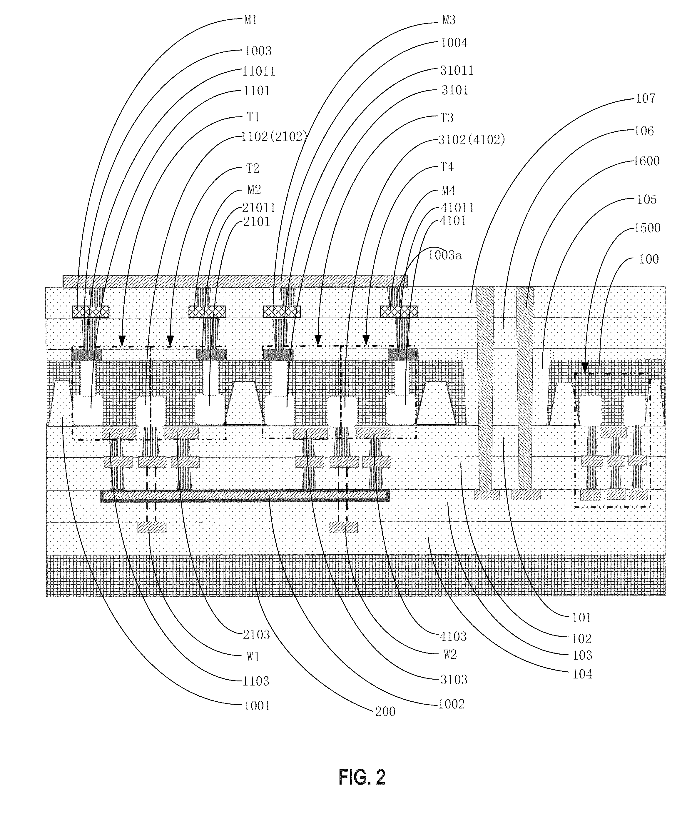
[0053]According to a second embodiment of the present invention, there is provided an integrated circuit. The integrated circuit includes an array of semiconductor memory control units, each of the control units includes a switching transistor having reduced coupling capacitance between the gate and drain due to the disposition of gate and drain on opposite sides of the substrate. Accordingly, the switching transistor has a reduced physical size and better performance.
[0054]FIG. 2 is a simplified cross-sectional view of an integrated circuit structure according to a second embodiment of the present invention. FIG. 3 is a simplified circuit diagram of FIG. 2. Although FIGS. 2 and 3 only show the integrated circuit having four semiconductor memory control units, it is understood that the number of semiconductor memory control units can be any integer number. It is understood that the number is arbitrary chosen for describing the example embodiment and should not be limiting. The terms...
third embodiment
[0072]A method for manufacturing an integrated circuit will be described according to an exemplary embodiment of the present invention. The method of manufacturing an integrated circuit according to a third embodiment of the present invention will be described below. For example, the integrated circuit structure of FIG. 2 can be formed by the following steps:
[0073]Step A1: providing a semiconductor substrate 100 having a first surface and an opposite second surface; and forming a thin stop layer having a first depth on the first surface of semiconductor substrate 100.
[0074]In an embodiment, the first surface of semiconductor substrate 100 denotes the surface that includes a gate electrode of a transistor, the second surface of semiconductor substrate 100 denotes the surface that is opposite the first surface, the depth of the stop layer is measured in reference to the first surface. The term “a layer having a first depth H1” denotes the distance H1 measured between the top surface o...
PUM
 Abstract
Description
Claims
Application Information