Optical modulator

a technology of optical modulators and modulators, applied in the field of optical modulators, can solve the problems of high half-wave voltage v, direct modulation has a limited modulation rate, and high-speed optical modulators have a length as long as approximately 10 cm, so as to reduce vl and efficiently apply

Active Publication Date: 2015-05-21
TDK CORPARATION
View PDF0 Cites 23 Cited by
  • Summary
  • Abstract
  • Description
  • Claims
  • Application Information

AI Technical Summary

Benefits of technology

[0010]The present invention provides an optical modulator that includes a single-crystal substrate, a lithium niobate film formed on a main surface of the single-crystal substrate, the lithium niobate film being an epitaxial film and having a ridge, a buffer layer formed on the ridge, a first electrode formed on the buffer layer, and a second electrode separated from the first electrode, the second electrode being in contact with the lithium niobate film. This structure allows an electric field to be efficiently applied to an optical waveguide and can decrease VπL while maintaining the characteristic impedance Zc of a traveling-wave electrode.

Problems solved by technology

Although the direct modulation needs no optical modulator and is inexpensive, the direct modulation has a limited modulation rate.
However, these high-speed optical modulators have the drawback of having a length as long as approximately 10 cm.
However, this optical modulator including the lithium niobate film has the following problems. FIG. 15 is a cross-sectional view of an optical modulator 100 described in Japanese Unexamined Patent Application Publication No. 2006-195383.
This causes the problem of a high half-wave voltage Vπ.
Although the half-wave voltage Vπ can be lowered by increasing the electrode length L, this results in an increased size.
Thus, the optical modulator has the problem of high VπL.

Method used


Image

  • Optical modulator
  • Optical modulator
  • Optical modulator

Examples


examples

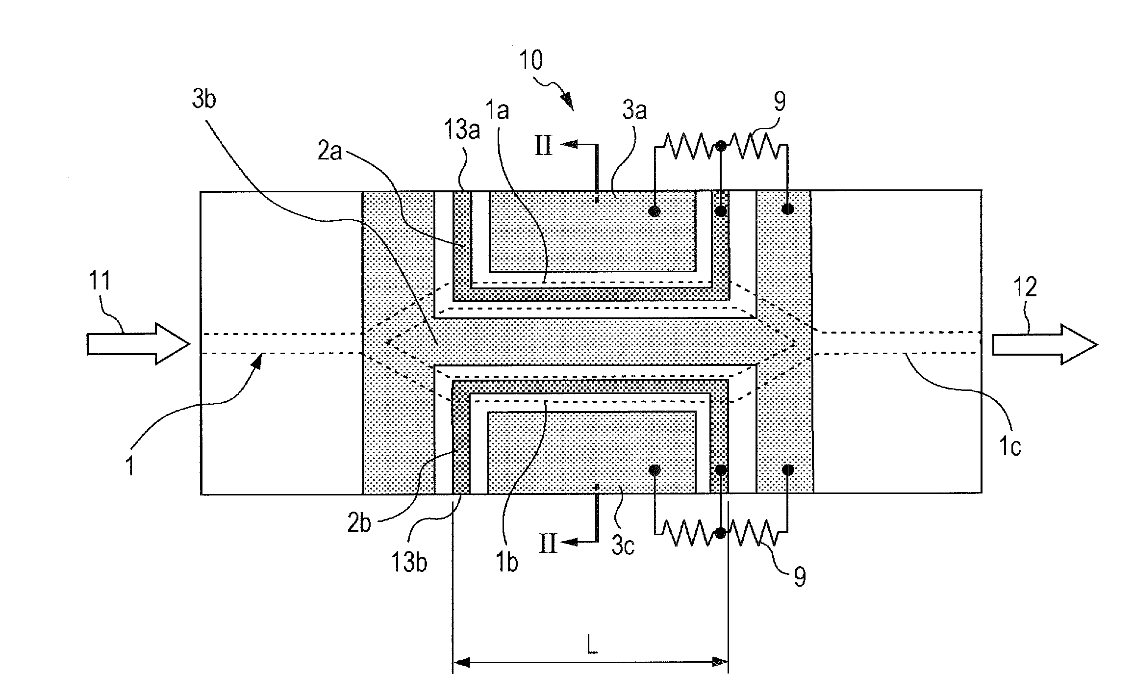
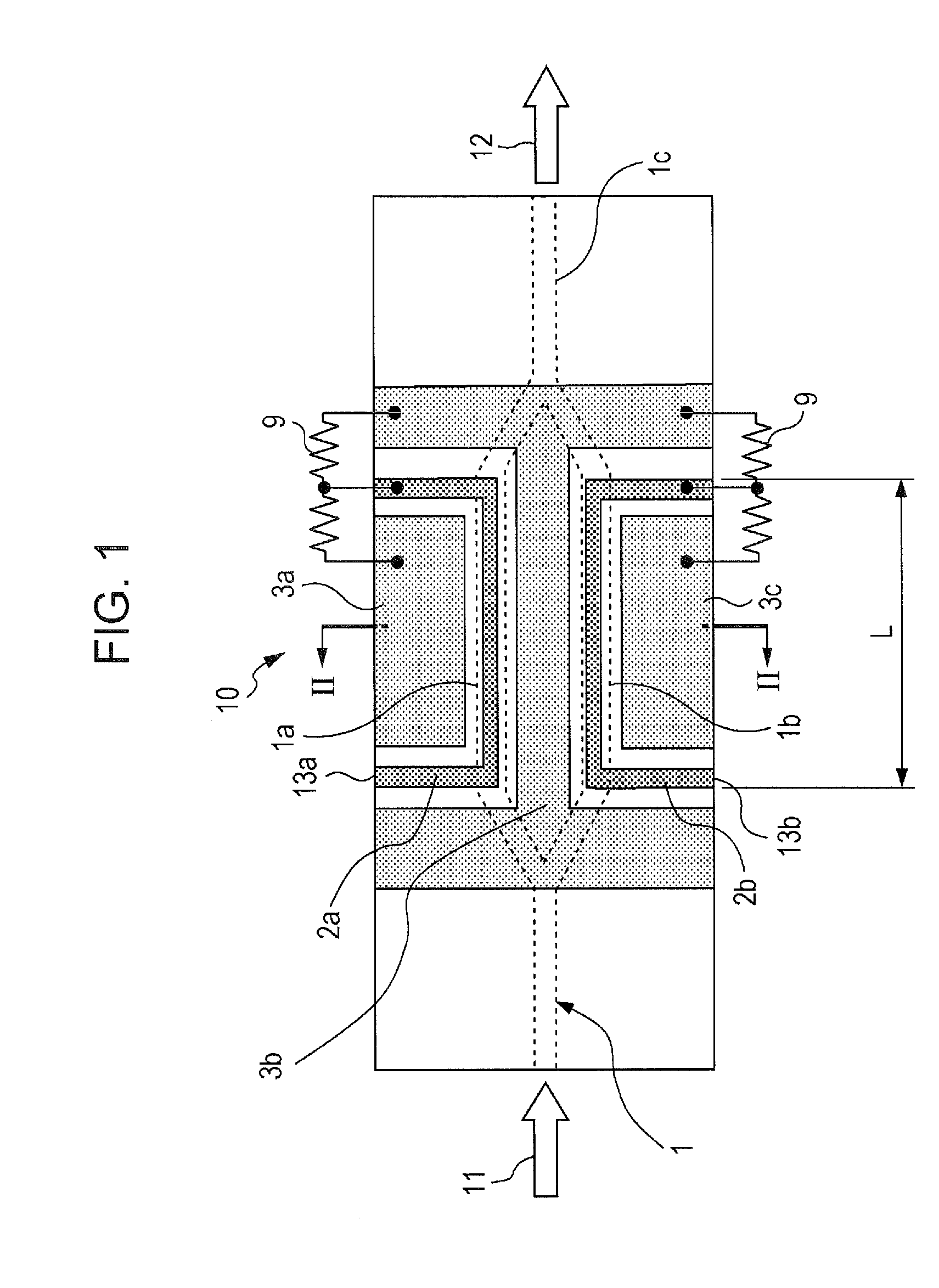
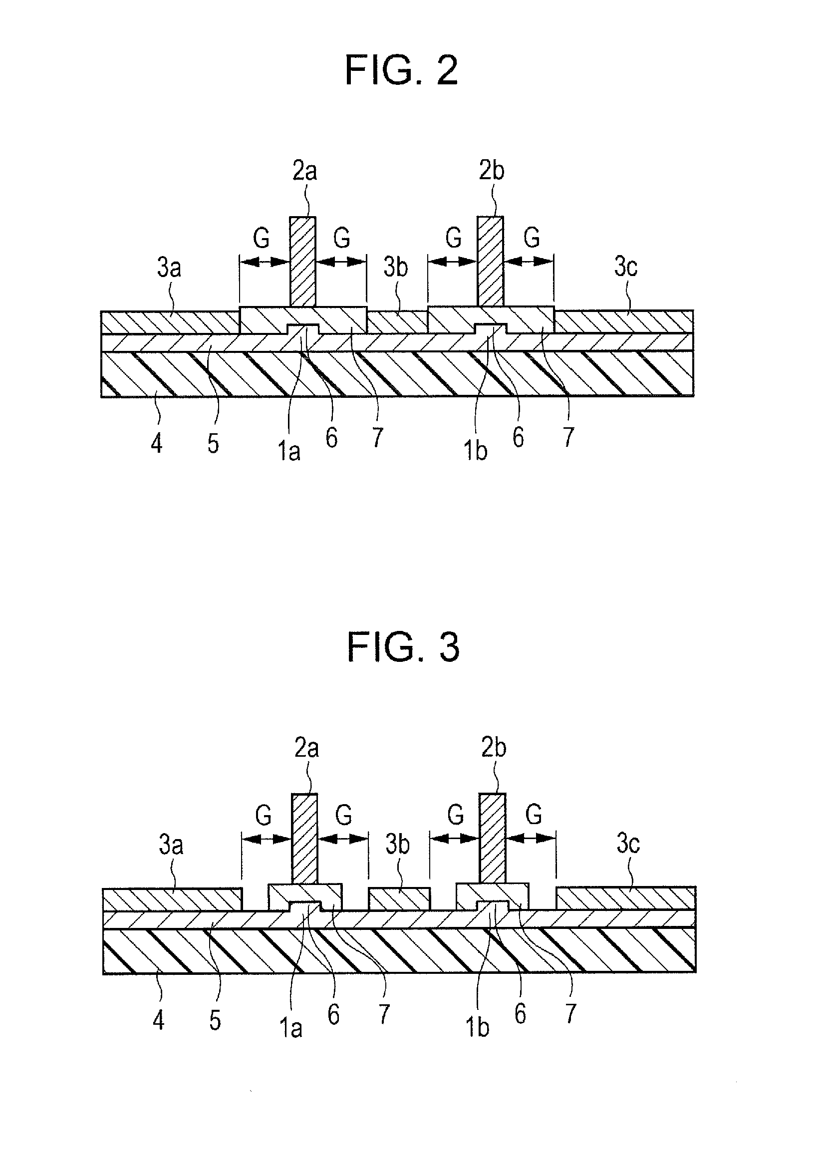
[0054]The structure according to the sixth embodiment illustrated in FIG. 13 was test-manufactured in accordance with the following procedures. The material of the single-crystal substrate 4 was sapphire. The lithium niobate film 5 having a thickness of 1.5 μm was formed by sputtering on the single-crystal substrate 4. The buffer layer 7 having a thickness of 0.8 μm and formed of LaAlO3 was then formed by vapor deposition on the lithium niobate film 5. The formation of the ridges 6 and patterning of the buffer layers were performed by the formation of a resist mask and Ar plasma dry etching. The ridges 6 had a width of 2.5 μm and a height of 0.4 μm. The dielectric layers 8 having a thickness of 0.7 μm and formed of SiO2 were formed by CVD over the entire surface. A resist mask was formed again, and an unnecessary portion of the dielectric layers 8 was removed by dry etching. Finally, the first electrodes 2a and 2b and the second electrodes 3a, 3b, and 3c were formed using a photo pr...


PUM

PropertyMeasurementUnit
relative dielectric constantaaaaaaaaaa
lengthaaaaaaaaaa

Abstract

An optical modulator includes a single-crystal substrate, a lithium niobate film formed on a main surface of the single-crystal substrate, the lithium niobate film being an epitaxial film and having a ridge, a buffer layer formed on the ridge, a first electrode formed on the buffer layer, and a second electrode separated from the first electrode, the second electrode being in contact with the lithium niobate film.

Description

BACKGROUND OF THE INVENTION[0001]1. Field of the Invention[0002]The present invention relates to an optical modulator for use in optical communication and optical measurement fields.[0003]2. Description of the Related Art[0004]With the spread of the Internet, communication traffic is increasing dramatically, and optical fiber communication is becoming very important. In optical fiber communication, electric signals are converted into optical signals, and the optical signals are transmitted through optical fibers. Optical fiber communication is characterized by broadband, low-loss signals with high resistance to noise.[0005]Electric signals are converted into optical signals by direct modulation using a semiconductor laser or external modulation using an optical modulator. Although the direct modulation needs no optical modulator and is inexpensive, the direct modulation has a limited modulation rate. Thus, external modulation is used in high-speed long-distance applications.[0006]In...

Claims


Application Information

Patent Timeline
Patent Type & Authority Applications(United States)
IPC IPC(8): G02F1/00G02F1/03
CPCG02F1/0316G02F1/0018G02F1/035G02F1/225G02F2201/07
Inventor IWATSUKA, SHINJISASAKI, KENJITANIGUCHI, MASAMICHI
Owner TDK CORPARATION
Why Eureka
Try Eureka