Single crystal silicon ingot and wafer, and apparatus and method for growing said ingot

Inactive Publication Date: 2015-05-28
LG SILTRON
View PDF0 Cites 9 Cited by
  • Summary
  • Abstract
  • Description
  • Claims
  • Application Information

AI Technical Summary

Benefits of technology

[0054]High-quality single-crystal silicon ingots and wafers for semiconductors according to embodiments may be formed to include a transition region having crystal defects smaller than 30 nm, for example, having a size of 10 nm to 19 nm because detection of micro crystal defects smaller than 30 nm may be accomplished using a Magics method. The high-quality single-crystal silicon ingots and wafers may be used in semiconductor devices having a reduced width of 20 nm or less.
[0055]In addition, apparatuses and methods of growing single-crystal silicon ingots according to embodiments may accomplish more accurate control of a pulling rate of a single-crystal silicon ingot because the pulling rate is controlled after stabilizing flow of

Problems solved by technology

Growth of single-crystal silicon ingots by FZ methods, however, has several problems, such as difficulty in manufacturing large-diameter silicon wafers and considerably expensive process costs.
However, the aforementioned conventional crystal defect evaluation methods provide detection of crystal defects greater than 30 nm and cannot properly eval

Method used


Image

  • Single crystal silicon ingot and wafer, and apparatus and method for growing said ingot
  • Single crystal silicon ingot and wafer, and apparatus and method for growing said ingot
  • Single crystal silicon ingot and wafer, and apparatus and method for growing said ingot

Examples


Embodiment Construction

[0071]Hereinafter, in order to describe the present invention embodiments will be described in detail with reference to the accompanying drawings to improve understanding of the present invention. However, various modifications of the embodiments are possible, and the technical sprit of the present invention is not constructed as being limited to the embodiments. The embodiments of the present invention are provided to explain the disclosure to those skilled in the art.

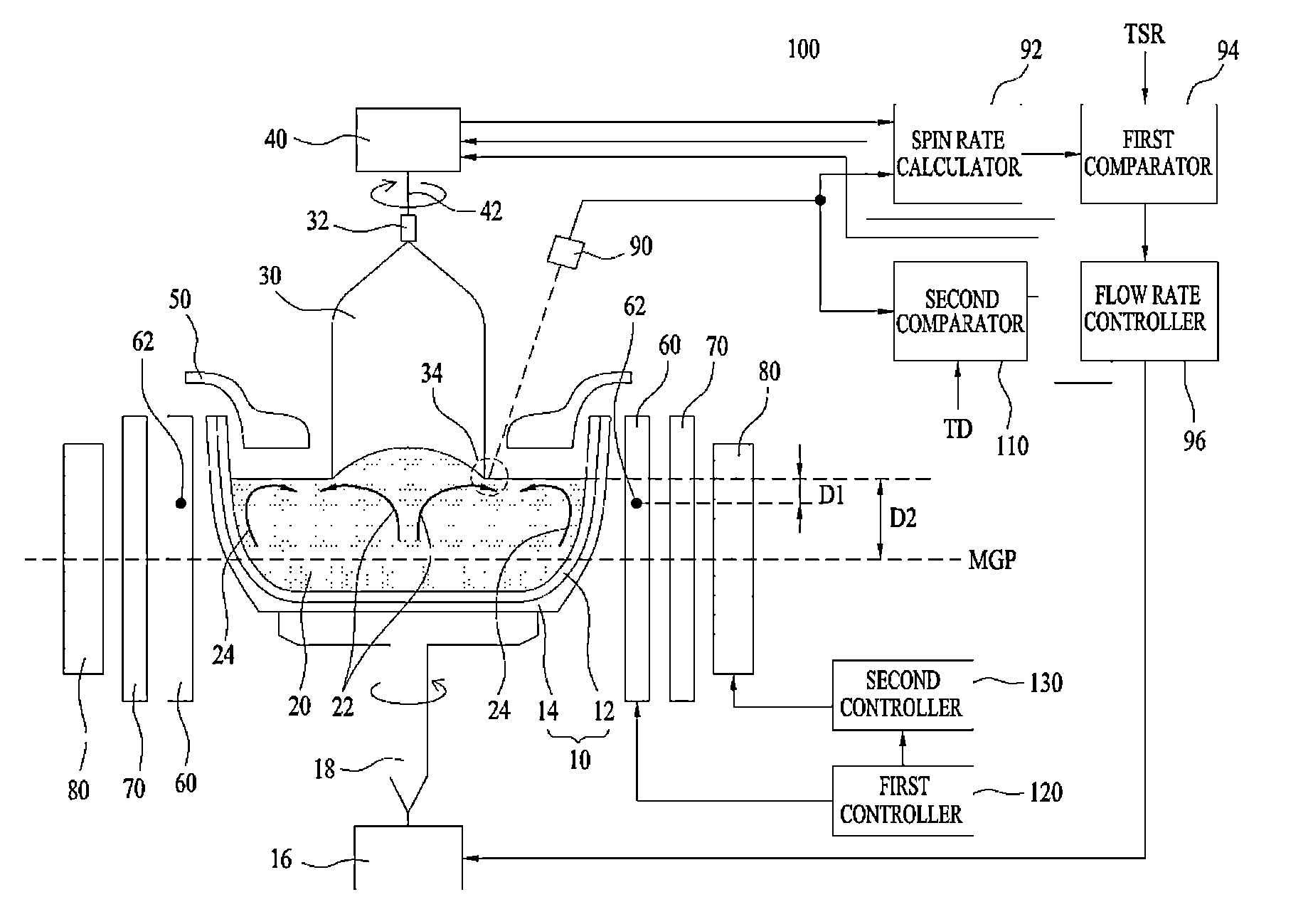
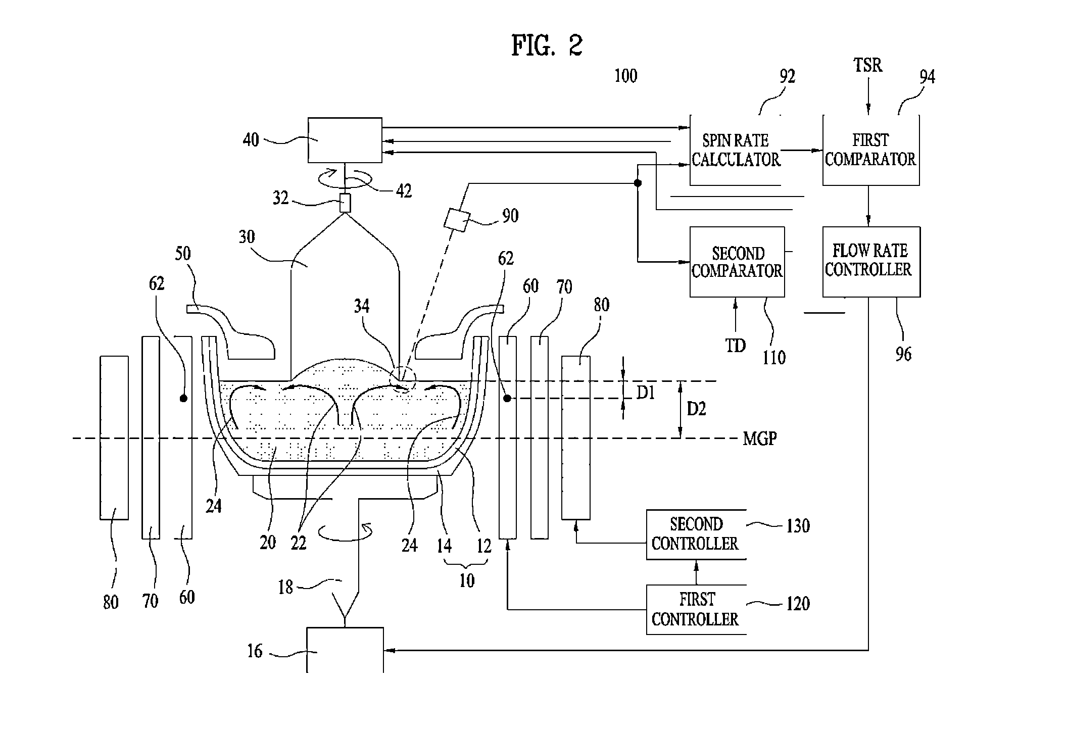
[0072]FIG. 2 is a view showing an apparatus of growing a single-crystal ingot, designated by reference numeral 100, according to an embodiment.

[0073]The single-crystal ingot growth apparatus 100 shown in FIG. 2 includes a crucible 10, a support shaft drive unit 16, a rotatable support shaft 18, a silicon melt 20, an ingot 30, a seed crystal 32, a wire hoist 40, a pull wire 42, a heat-shield member 50, a heater 60 arranged around the crucible 10, an insulator 70, a magnetic field generator 80, a diameter sensor 90, a s...


PUM


Abstract

The single crystal silicon ingot and wafer of one embodiment has a transition region formed therein which predominantly has crystal defects of 10 nm to 30 nm in size from among crystal defects included in at least one region of a vacancy predominant non-defective region and an interstitial predominant non-defective region.

Description

TECHNICAL FIELD[0001]Embodiments relate to single-crystal silicon ingots and wafers, and apparatuses and methods of growing the ingots.BACKGROUND ART[0002]General frequently used methods of manufacturing silicon wafers include Floating Zone (“FZ”) or CZochralski (“CZ”) methods. Growth of single-crystal silicon ingots by FZ methods, however, has several problems, such as difficulty in manufacturing large-diameter silicon wafers and considerably expensive process costs. Therefore, growth of single-crystal silicon ingots by CZ methods is prevalent.[0003]With such a CZ method, after polycrystalline silicon is charged into a quartz crucible and molten via heating of a graphite heating element, a seed crystal is dipped into the resulting silicon melt to cause crystallization at an interface of the silicon melt and then pulled while being rotated, thereby completing growth of a single-crystal silicon ingot. Thereafter, the grown single-crystal silicon ingot is subjected to slicing, etching...

Claims


Application Information

Patent Timeline
IPC IPC(8): C30B29/06C30B30/04C30B15/14
CPCC30B29/06C30B30/04C30B15/14C30B15/00C30B15/20Y10T117/1068
Inventor HONG, YOUNG HOHWANG, JUNG HACHA, IL SEON
Owner LG SILTRON
Why Eureka
Try Eureka