
Graphene, graphene-including layer, electrode, and power storage device

a graphene and electrode technology, applied in the direction of conductive materials, primary cells, secondary cells, etc., can solve the problems of difficult to efficiently increase only the weight of active materials, difficult to increase the charge and discharge capacity per unit weight or volume of electrodes, and electrodes are likely to be deformed and broken. , to achieve the effect of increasing the charge and discharge capacity, improving reliability and endurance, and high conductivity

Inactive Publication Date: 2015-06-18
SEMICON ENERGY LAB CO LTD
View PDF2 Cites 29 Cited by
  • Summary
  • Abstract
  • Description
  • Claims
  • Application Information

AI Technical Summary

Benefits of technology

The invention aims to provide a power storage device with high charge and discharge capacity per unit weight of an electrode, high reliability, and durability. The invention also provides a method for fabricating the power storage device. Additionally, the invention includes graphene with higher conductivity than traditional methods, and a novel material, electrode, and power storage device. The patent is about identifying and addressing issues with current power storage devices and proposing a solution to improve their performance.

Problems solved by technology

For this reason, it is difficult to efficiently increase only the weight of the active material in the electrode included in the power storage device, and thus, it is difficult to increase the charge and discharge capacity per unit weight or volume of the electrode.
Furthermore, the electrode included in the power storage device also has a problem in that the binder included in the active material layer swells as it comes into contact with an electrolytic solution, so that the electrode is likely to be deformed and broken.

Method used


Image

  • Graphene, graphene-including layer, electrode, and power storage device
  • Graphene, graphene-including layer, electrode, and power storage device
  • Graphene, graphene-including layer, electrode, and power storage device

Examples


embodiment 1

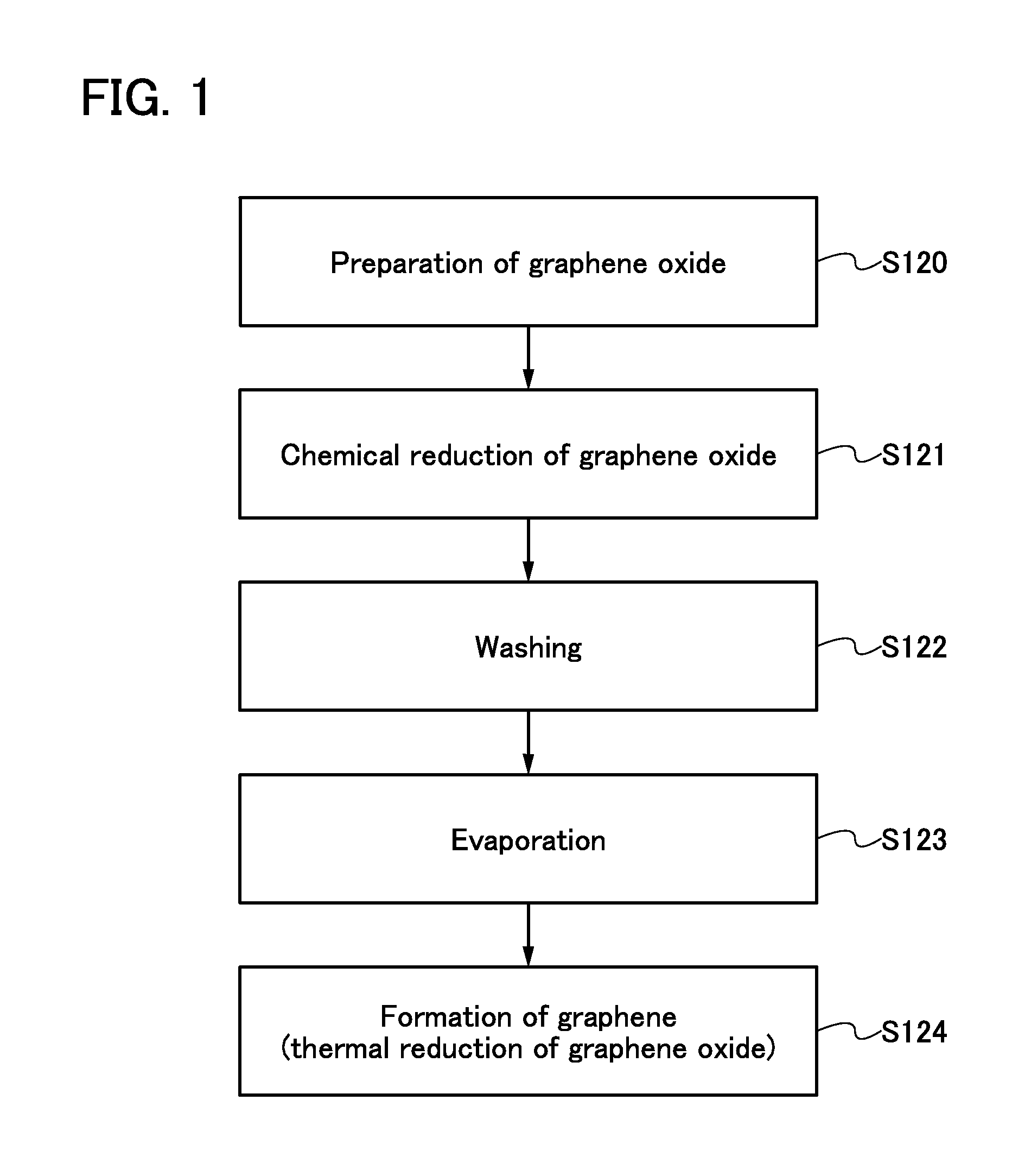
[0048]A method for forming graphene of one embodiment of the present invention and the physical properties of graphene formed by the method for forming graphene will be described. FIG. 1 shows steps for forming graphene. In this embodiment, an example of forming graphene will be described.

[0049]One embodiment of the present invention is a method for forming graphene by performing chemical reduction and thermal reduction on graphene oxide in this order.

120>

[0050]In Step S120 in FIG. 1, graphene oxide is prepared.

[0051]Graphene oxide is a raw material of graphene. Graphene oxide can be formed by various synthesis methods such as a Hummers method, a modified Hummers method, and oxidation of graphite.

[0052]For example, in a Hummers method, graphite such as flake graphite is oxidized to give graphite oxide. The obtained graphite oxide is graphite that is oxidized in places and thus to which a functional group such as a carbonyl group, a carboxyl group, or a hydroxyl group is bonded. In t...

embodiment 2

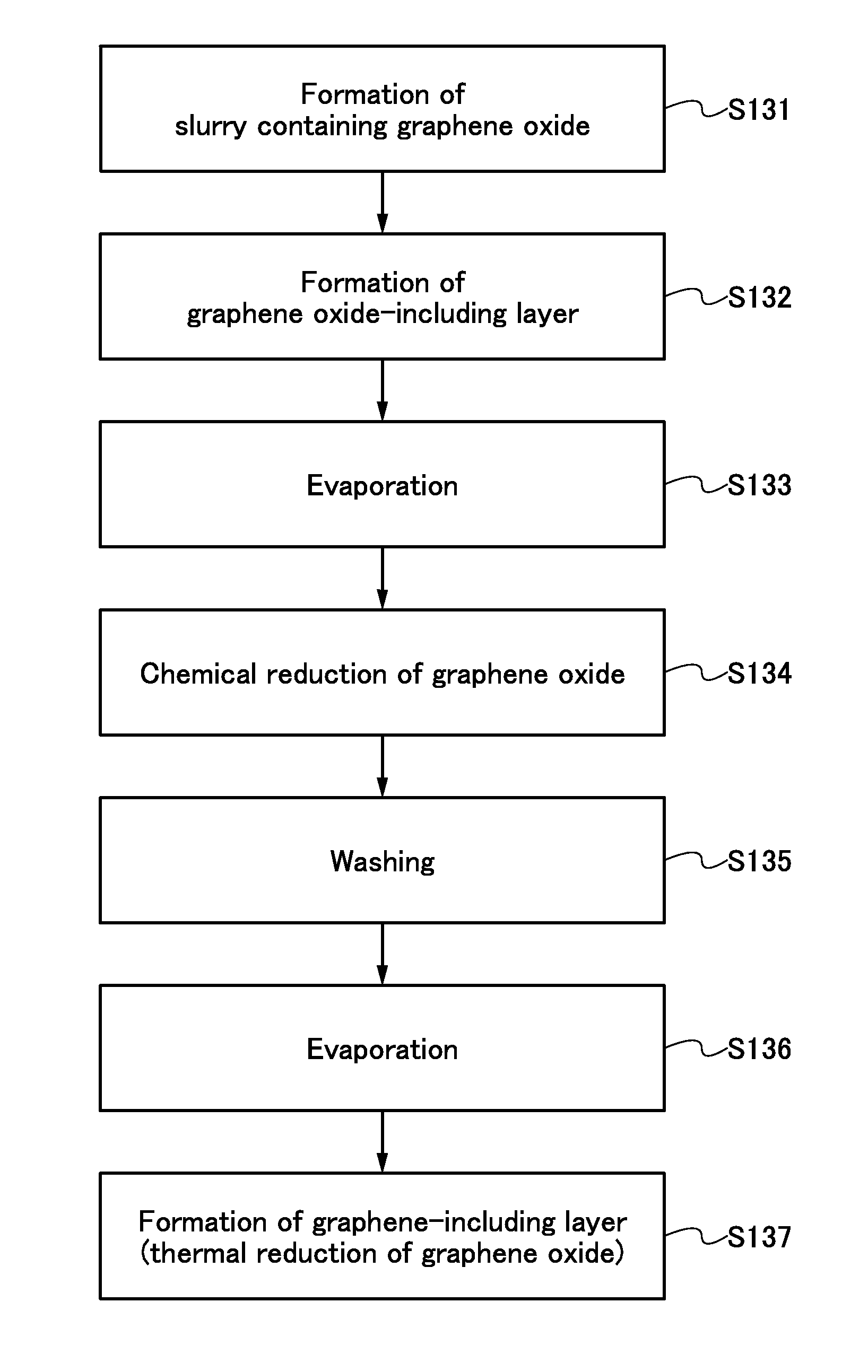
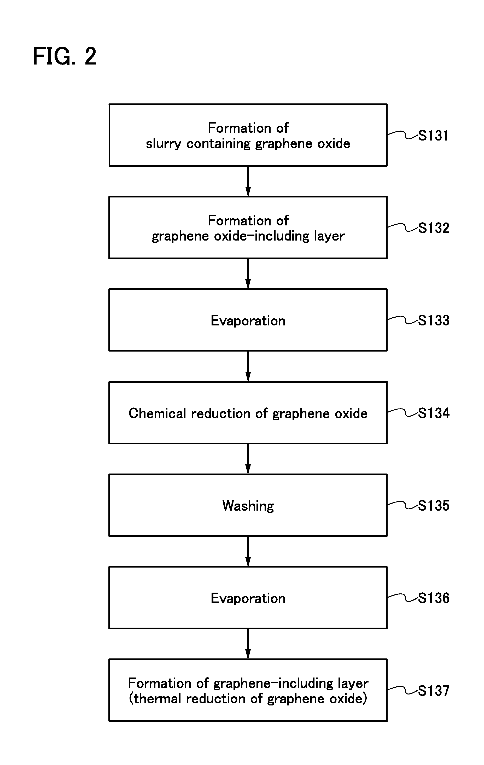
[0068]A method for forming a graphene-including layer of one embodiment of the present invention and the physical properties of a graphene-including layer formed by the method will be described. FIG. 2 shows steps for forming a graphene-including layer. In this embodiment, an example of forming a graphene-including layer from a graphene oxide-including layer will be described.

[0069]One embodiment of the present invention is a method for forming a graphene-including layer by performing chemical reduction and thermal reduction on a graphene oxide-including layer in this order.

131>

[0070]Slurry containing graphene oxide is formed in Step S131 in FIG. 2. The “slurry” refers to a suspension in which a material and a solvent are mixed. For example, in the case where a graphene-including layer is used for a positive electrode or a negative electrode of a power storage device, the slurry can contain an active material, a solvent, and the like in addition to the graphene oxide. The slurry can...

embodiment 3

[0093]In this embodiment, an electrode of one embodiment of the present invention will be described with reference to FIGS. 3A and 3B. Specifically, an electrode fabricated using the method for forming graphene that is described in Embodiment 1 or the method for forming a graphene-including layer that is described in Embodiment 2 will be described.

[0094]In this embodiment, an example of using the electrode of one embodiment of the present invention as one or both of a positive electrode and a negative electrode of a power storage device will be described. Specifically, an electrode (a positive electrode or a negative electrode) fabricated using a method for forming a graphene-including active material layer by forming an active material layer including an active material and graphene oxide over a current collector and performing chemical reduction and thermal reduction on the graphene oxide in this order will be described.

[0095]FIG. 3A is a cross-sectional view of an electrode 100, ...


PUM


Abstract

Graphene that is formed from graphene oxide and has high conductivity and a method for forming the graphene are provided. A power storage device with high charge discharge capacity and favorable electric properties such as high reliability and high durability and a method for fabricating the power storage device are provided. Chemical reduction and thermal reduction are performed on graphene oxide in this order to form graphene. In the method for fabricating the power storage device including at least a positive electrode, a negative electrode, an electrolytic solution, and a separator, graphene of one or both of a positive electrode and a negative electrode is formed by the forming method of graphene.

Description

BACKGROUND OF THE INVENTION[0001]1. Field of the Invention[0002]Embodiments of the present invention relate to a forming method of graphene and fabricating methods of an electrode including the graphene and a power storage device including the electrode. Embodiments of the present invention relate to graphene formed by the forming method and an electrode and a power storage device fabricated by the fabricating method. Note that a power storage device in this specification refers to every element and / or device having a function of storing electric power, such as a lithium primary battery, a lithium-ion secondary battery, or a lithium-ion capacitor. Note that one embodiment of the present invention is not limited to the above technical field. The technical field of one embodiment of the invention disclosed in this specification and the like relates to an object, a method, or a fabricating method. In addition, one embodiment of the present invention relates to a process, a machine, man...

Claims


Application Information

Patent Timeline
IPC IPC(8): C01B31/04H01M4/58H01M4/04H01M4/1393H01G11/06H01G11/32H01G11/86H01M4/62H01M6/00H01M50/103H01M50/105H01M50/107H01M50/109H01M50/119H01M50/121H01M50/129
CPCC01B31/0438H01M4/625H01M4/5825C01B31/0446H01M4/049H01M4/1393H01M4/0404H01M6/00H01G11/06H01G11/32H01G11/86H01M4/0471H01G11/34H01G11/50H01M4/1397H01M10/052H01M10/0525H01M2220/20H01M2220/30C01B32/182C01B32/184C01B32/198H01M50/109H01M50/105H01M50/129H01M50/107H01M50/119H01M50/103H01M50/121H01M4/133C01B2204/22Y02E60/13Y02E60/10Y02P70/50
Inventor IKENUMA, TATSUYAYUKAWA, MIKIO
Owner SEMICON ENERGY LAB CO LTD
Learn More