Cascode amplifier

Active Publication Date: 2015-06-18
MURATA MFG CO LTD
View PDF1 Cites 3 Cited by
  • Summary
  • Abstract
  • Description
  • Claims
  • Application Information

AI Technical Summary

Benefits of technology

[0006]In the case of a cascode amplifier made up of CMOS as well as an amplifier made up of GaAs HBT, it is also possible to prevent deterioration of power added efficiency when output power decreases by controlling the supply voltage using a DC-DC converter. However, since output impedance drastically changes at a point of operation at which a gat

Problems solved by technology

However, since output impedance drastically changes at a point of operation at which a gate-grounded transistor transitions from saturation operation to linear operation, an output signal is distorted.
However, since the operation range of the d

Method used


Image

  • Cascode amplifier
  • Cascode amplifier
  • Cascode amplifier

Examples


Example

First Embodiment

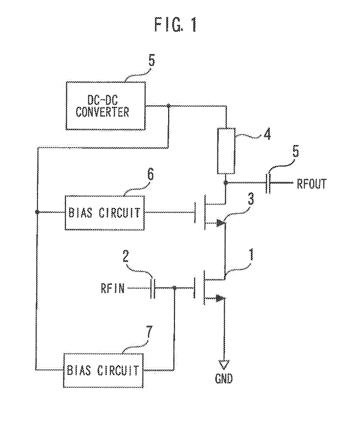
[0018]FIG. 1 is a diagram illustrating a cascode amplifier according to a first embodiment of the present invention. A transistor 1 is a source-grounded transistor that has a gate, a grounded source and a drain. A signal is inputted to the gate of the transistor 1 via a DC cut capacitance 2.

[0019]A transistor 3 is a gate-grounded transistor that includes a gate, a source connected to the drain of the transistor 1 and a drain. A load 4 is connected to the drain of the transistor 3. A signal is outputted from the drain of the transistor 3 via a DC cut capacitance 5. The transistors 1 and 3 are silicon MOSFETs.

[0020]A DC-DC converter 5 supplies a supply voltage which is variable according to output power to the drain of the transistor 3 via the load 4. A bias circuit 6 supplies a voltage expressed by a function of the supply voltage to the gate of the transistor 3. A bias circuit 7 supplies a voltage expressed by a function of the supply voltage to the gate of the trans...

Example

Second Embodiment

[0027]FIG. 4 is a diagram illustrating a cascode amplifier according to a second embodiment of the present invention. A low pass filter 11 is connected between the input of the bias circuit 6 and the drain of the transistor 3. Furthermore, the bias circuit 7 supplies a voltage expressed by a function of the output voltage of the bias circuit 6 to the gate of the transistor 1.

[0028]Since it is difficult to integrate the cascode amplifier and the DC-DC converter 5 on the same chip, they are formed on different chips. Therefore, in the first embodiment, independent terminals to monitor the supply voltage are necessary, which may cause an increase of the chip size of the cascode amplifier and an increase of mounting area when the DC-DC converter 5 is combined. Thus, in the present embodiment, the input of the bias circuit 6 is connected to the drain of the transistor 3. This eliminates the necessity for providing additional terminals and can prevent the chip size and mo...

Example

Third Embodiment

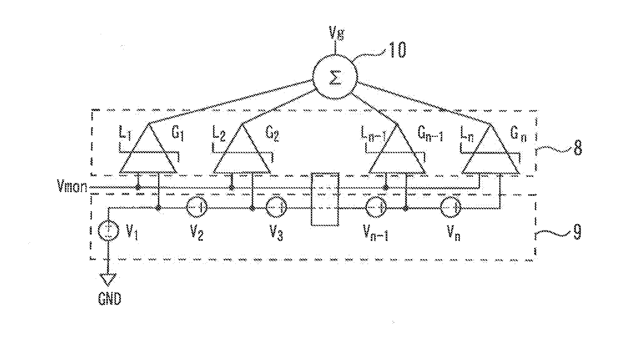
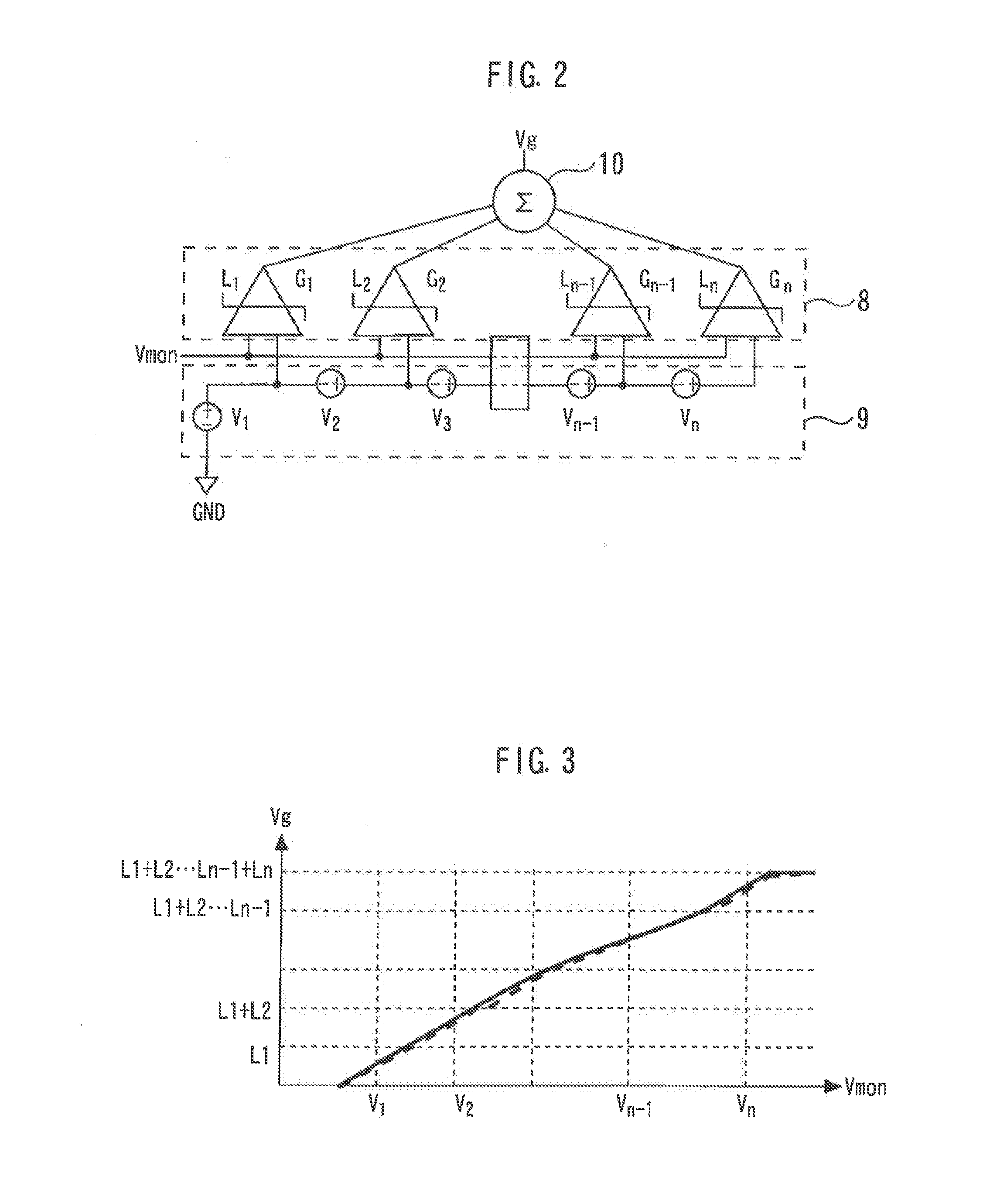
[0030]FIG. 5 is a diagram illustrating a cascode amplifier according to a third embodiment of the present invention. A digital interface 12 receives a digital signal from outside and decodes the digital signal. Memories 13 and 14 store digital information inputted from outside. Functions of the bias circuits 6 and 7 are set according to digital information stored in the memories 13 and 14. This allows optimum conditions to be set for control conditions of the DC-DC converter 5 and bias conditions of the cascode amplifier which vary depending on differences in a modulation scheme or the like, making it possible to obtain excellent power added efficiency for various operation conditions.

[0031]FIG. 6 is a diagram illustrating a bias circuit according to the third embodiment of the present invention. A reference voltage Vi (i=1 . . . n), a gain Gi (i=1 . . . n), and a limiting level Li (i=1 . . . n) of each of a plurality of limiter amplifiers 8 and a plurality of refere...


PUM


Abstract

A cascode amplifier includes: a first transistor having a gate to which a signal is input, a grounded source, and a drain; a second transistor having a gate, a source connected to the drain of the first transistor, and a drain; a load connected to the drain of the second transistor; a DC-DC converter supplying a supply voltage, which is variable according to output power, to the drain of the second transistor via the load; and a first bias circuit supplying a voltage, which is a function of the supply voltage, to the gate of the second transistor.

Description

BACKGROUND OF THE INVENTION[0001]1. Field of the Invention[0002]The present invention relates to a cascode amplifier made up of silicon CMOS of relatively low manufacturing cost, and more particularly, to a cascode amplifier with an expanded range of supply voltage control and capable of preventing deterioration of power added efficiency.[0003]2. Background Art[0004]Elements using processes of GaAs HBT or the like of good high-frequency characteristics and a high withstand voltage are generally used for high output amplifiers for amplification of transmission signals used for mobile communication devices such as mobile phones. High output amplifiers manufactured through these processes are designed to achieve maximum power added efficiency at maximum output power and the power added efficiency drastically deteriorates when output power decreases. A method of preventing efficiency deterioration when output power decreases is available which controls a supply voltage of a high output ...

Claims


Application Information

Patent Timeline
IPC IPC(8): H03F1/02H03F3/21
CPCH03F1/0211H03F2200/18H03F3/21H03F1/223H03F3/195H03F3/245
Inventor TAKAHASHI, YOSHINORIMIYASHITA, MIYOYAMAMOTO, KAZUYA
Owner MURATA MFG CO LTD
Why Eureka
Try Eureka